Ceramic raw wafer manufacturing method and multilayer ceramic electronic parts manufacturing method
A technology of ceramic green sheets and multi-layer ceramics, applied in the field of multi-layer ceramic electronic components and the manufacture of multi-layer ceramic electronic components, can solve the problems of electrode step delamination, extension electrode bending, short-circuit failure, etc., to improve durability, reduce Effect of small surface roughness
- Summary
- Abstract
- Description
- Claims
- Application Information
AI Technical Summary
Problems solved by technology
Method used
Image
Examples
no. 1 example
[0100] In this example, the fabrication of a ceramic green sheet for forming a dielectric layer of a monolithic ceramic capacitor is described as an example.
[0101] (1) First, a predetermined amount of ceramic powder (barium titanate ceramic powder) as a raw material and an additive for improving properties are weighed and mixed at a humidity level to form a mixed powder. Each additive is added to the ceramic powder in the form of oxide powder or carbonate powder, and the resulting mixture is wet-distributed in an organic solvent (dispersion solvent).
[0102] As a method of wet distribution (primary spreading), it is preferable to select a spreading method or spreading conditions in which ceramic powder is not ground. That is, it is preferable to disperse under the condition that the generated shearing force does not cause grinding.
[0103] Examples of the dispersion method include a ball milling method, a sand mixing method, a stick milling method, a high-pressure homoge...
no. 2 example
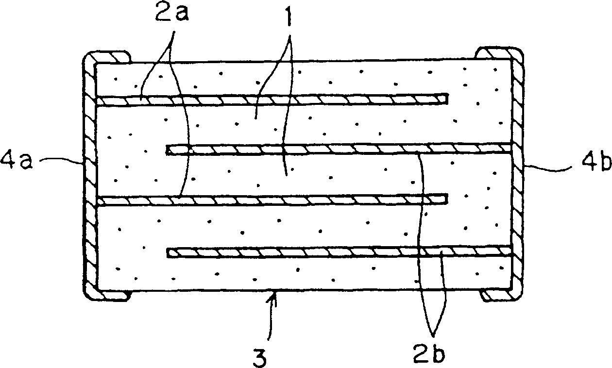
[0230] In this example, describe Figure 5 Fabrication of monolithic ceramic capacitors of the structure shown.
[0231] Figure 5 The monolithic ceramic capacitor 1 is a sheet-like monolithic ceramic capacitor, in its structure, a rectangular laminate 3 includes a ceramic layer 2 serving as a dielectric layer and alternately stacked first and second internal electrodes 8 and 9 , the first and second external electrodes 6 and 7 are disposed on the first and second end faces 4 and 5 of the laminate 3, and are connected to the first and second internal electrodes 8 and 9, respectively. On the external electrodes 6 and 7, first plating layers 10 and 11 and second plating layers 12 and 13 are formed, respectively.
[0232] A method of manufacturing a monolithic ceramic capacitor is described below.
[0233] (1) First, the raw material of dielectric ceramics, a predetermined amount of ceramic raw material powder such as barium titanate, and additives for improving properties are...
PUM
| Property | Measurement | Unit |
|---|---|---|
| surface roughness | aaaaa | aaaaa |
| thickness | aaaaa | aaaaa |
| thickness | aaaaa | aaaaa |
Abstract
Description
Claims
Application Information


