

Ion implantation method for generating window on dielectric layer
A technology of ion implantation and ion implantation area, which is applied in the manufacture of circuits, electrical components, semiconductors/solid-state devices, etc., and can solve problems such as inability to use manufacturing processes and non-straight contours
- Summary
- Abstract
- Description
- Claims
- Application Information
AI Technical Summary
Problems solved by technology
Method used
Image

Examples
Embodiment Construction
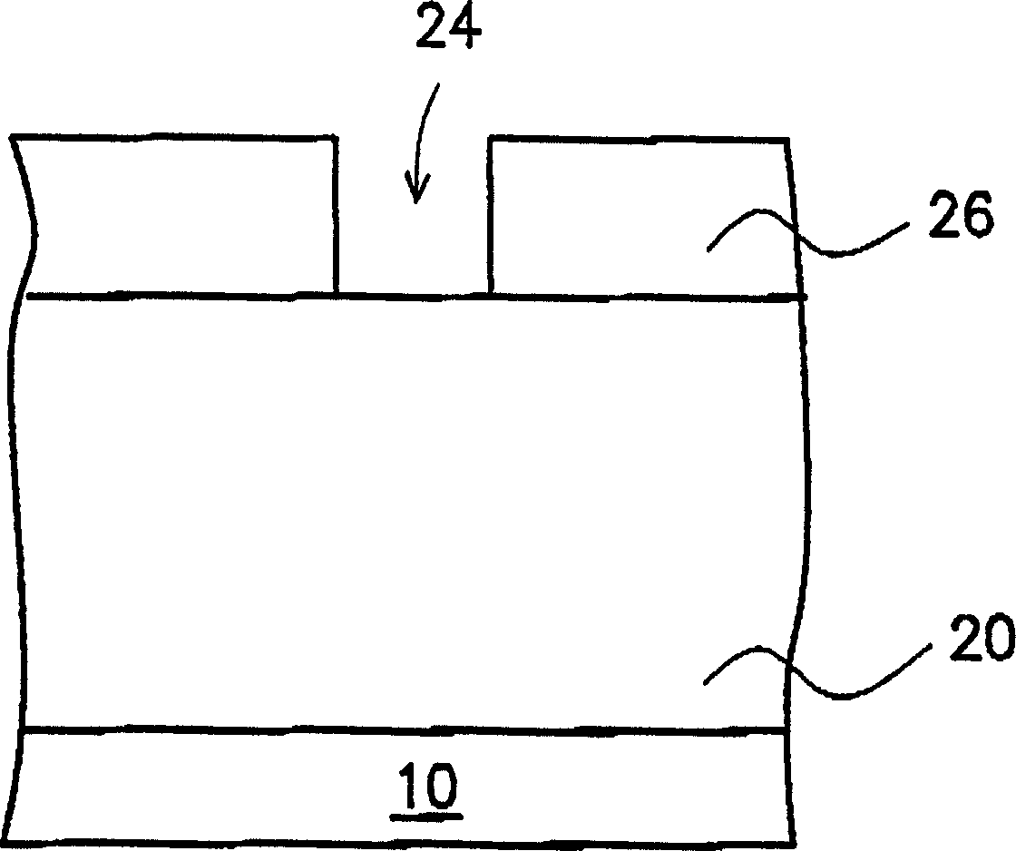
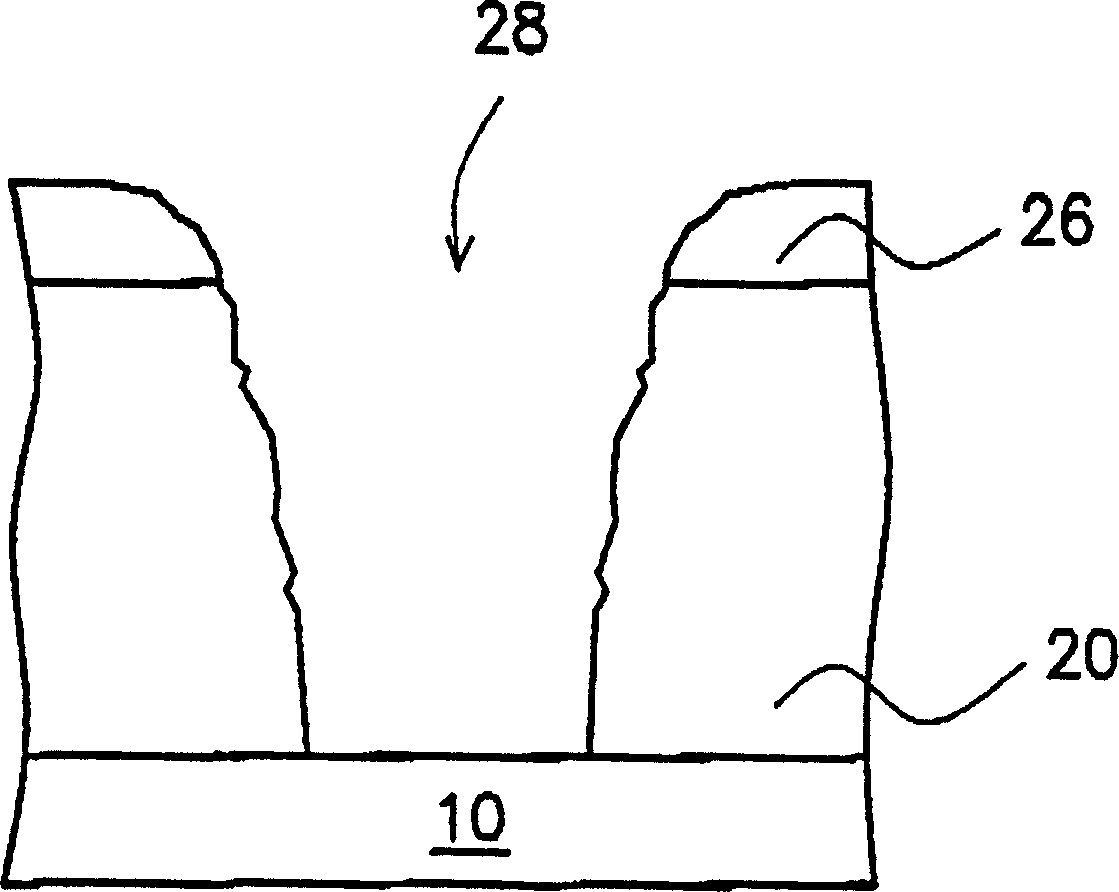
[0028] The present invention provides a method for forming openings in a dielectric layer by ion implantation. The dielectric layer includes, for example, at least one dielectric layer, and the upper layer is an ion-free dielectric layer. Now the photoresist layer is used as the mask layer, hydrogen fluoride is used as the chemical vapor phase etching gas, the ion-free oxide layer is used as the ion-free dielectric layer, and the ion-containing oxide layer is used as the ion-containing dielectric layer. Example. Wherein, the photoresist etching rate of this hydrogen fluoride vapor phase etching is small, such as less than 50 angstroms / minute, preferably less than 10 angstroms / minute, and the selectivity ratio of photoresist is large, such as greater than 20, preferably greater than 80.
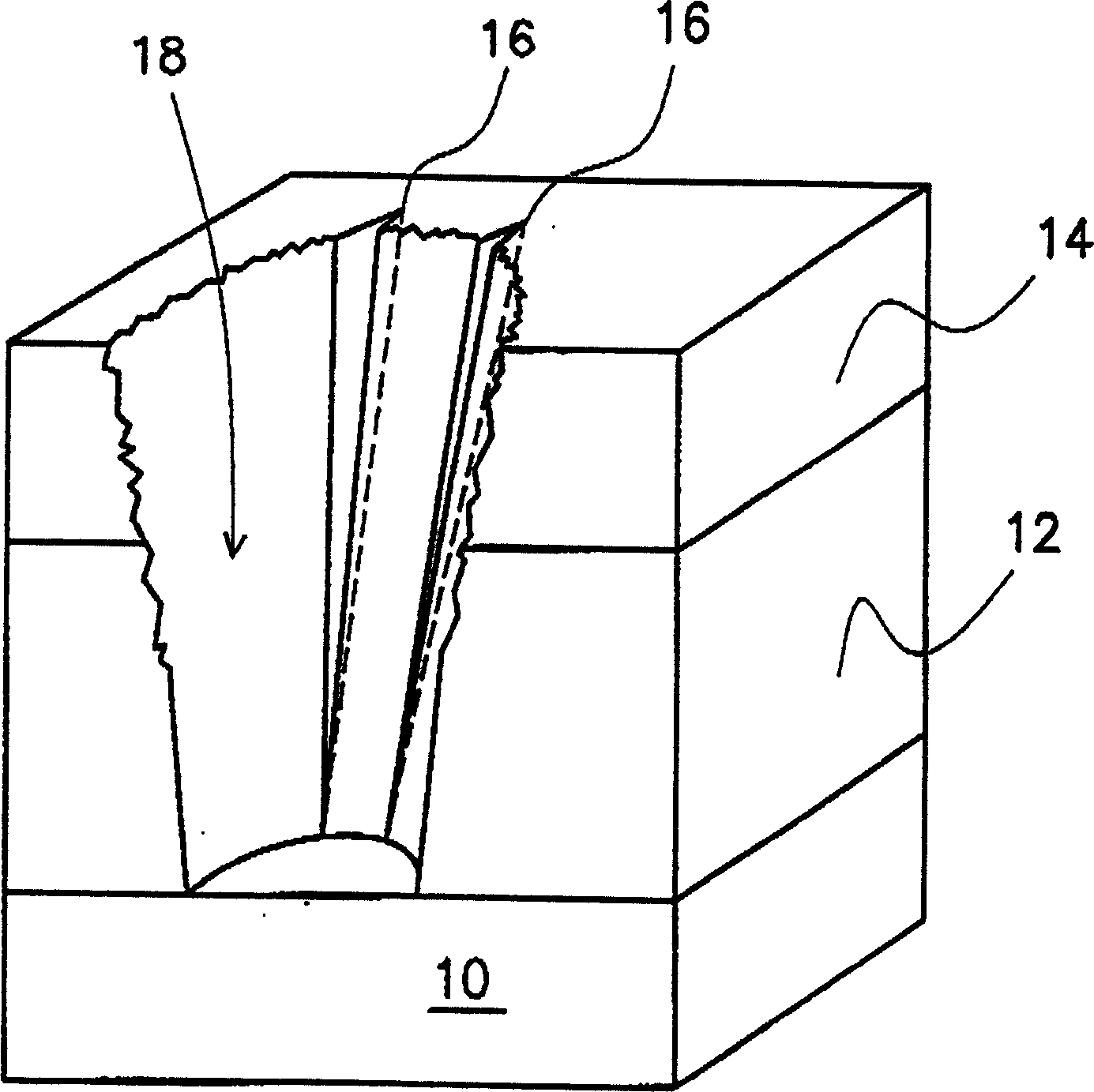
[0029] Figure 3A to Figure 3E , is a schematic cross-sectional view of the process flow of the method for forming openings in the dielectric layer by ion implantation according to the prese...
PUM
 Abstract
Description
Claims
Application Information