
Alloy plating liquid for modular printed circuit board surface treatment

A printed circuit board and surface treatment technology, applied in the secondary processing of printed circuits, printed circuits, printed circuit manufacturing, etc., can solve the problems of low economic efficiency and low productivity

Inactive Publication Date: 2006-03-15
SAMSUNG ELECTRO MECHANICS CO LTD +1
View PDF3 Cites 0 Cited by
  • Summary
  • Abstract
  • Description
  • Claims
  • Application Information

AI Technical Summary

Problems solved by technology

[0010] However, the conventional surface treatment methods for modular PCBs mentioned above have the disadvantages of low economic benefit and low productivity due to the complicated process of exposing the dry film, developing and delaminating the additional steps in the hard gold plating process

Method used


Image

  • Alloy plating liquid for modular printed circuit board surface treatment
  • Alloy plating liquid for modular printed circuit board surface treatment
  • Alloy plating liquid for modular printed circuit board surface treatment

Examples


Embodiment 1

[0043] Prepare an aqueous alloy plating solution having the composition shown in Table 1 below, and then activate the electroless nickel-plated modular PCB with 3% hydrochloric acid solution at 25° C. for 1 minute. While adjusting the temperatures of the three plating solution baths to 60°C, 70°C and 80°C, the PCB was immersed in the plating solution for 10 minutes for plating. As such, the plating solution was not stirred and the pH of the plating solution was 4.5.

[0044] Table 1

[0045] Element

content

Methanesulfonic acid

30g / l

sodium cyanide

10g / l

Thiourea

10g / l

Silver nitrate

0.25g / l

Potassium gold cyanide

5g / l

Nitriloacetic acid

3g / l

[0046] After the plating process, the board was washed with water, dried at 80° C. for 15 minutes, and then solderability and wear resistance were measured by the following conditions and methods.

[0047] - Solderability

[0048] The p...

Embodiment 2

[0059] Prepare an aqueous alloy plating solution having the composition shown in Table 3 below, and then use 3% hydrochloric acid solution at 25° C. to activate the electroless nickel plating layer of the electroless nickel-plated modular PCB for 1 minute. The plating process was performed using a plating solution at 80° C. at plating time periods of 5 minutes, 10 minutes, and 15 minutes. At this time, the plating solution was not stirred, and the pH of the plating solution was 4.5.

[0060] table 3

[0061] Element

content

Methanesulfonic acid

50g / l

potassium cyanide

10g / l

Thioglycolic acid

10g / l

Silver nitrate

0.25g / l

Potassium gold cyanide

5g / l

nitrilotriacetic acid

3g / l

[0062] Then, post-processing was performed in the same manner as in Example 1, and solderability and wear resistance were measured. The results are shown in Table 4 below.

[0063] period

Embodiment 3

[0065] Prepare an aqueous alloy plating solution having the composition shown in Table 5 below, and then use 3% hydrochloric acid solution at 25° C. to activate the electroless nickel-plated modular PCB for 1 minute. Then, the plating process was performed for 10 minutes using a plating solution at 80° C., and the stirring conditions were 0.1 m / s, 0.2 m / s, and 0.3 m / s, respectively.

[0066] table 5

[0067] Element

content

Methanesulfonic acid

40g / l

potassium cyanide

6g / l

Methylthiourea

1.5g / l

silver cyanide

0.1g / l

Potassium gold cyanide

2.5g / l

DTPA-5Na

3g / l

[0068] Then, post-processing was performed in the same manner as in Example 1, and solderability and wear resistance were measured. The results are shown in Table 6 below.

[0069] to stir


PUM

PropertyMeasurementUnit
thicknessaaaaaaaaaa
thicknessaaaaaaaaaa
sizeaaaaaaaaaa

Abstract

Disclosed is an aqueous alloy plating solution for surface treatment of a modular PCB. The plating solution comprises 1-30 wt % of an organic acid having at least one sulfonic acid group (-SO3H), 0.1-20 wt % of a complexing agent, 0.1-15 wt % of a thio-compound having at least one -S-, 0.05-5 wt % of a water soluble gold compound, 0.001-1 wt % of a water soluble silver compound and 0.1-10 wt % of a sequestering agent, based upon the weight of the plating solution. According to this invention, all plating properties required for the modular PCB are obtained through a single plating process, instead of the conventional double plating process.

Description

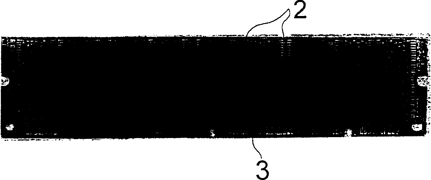
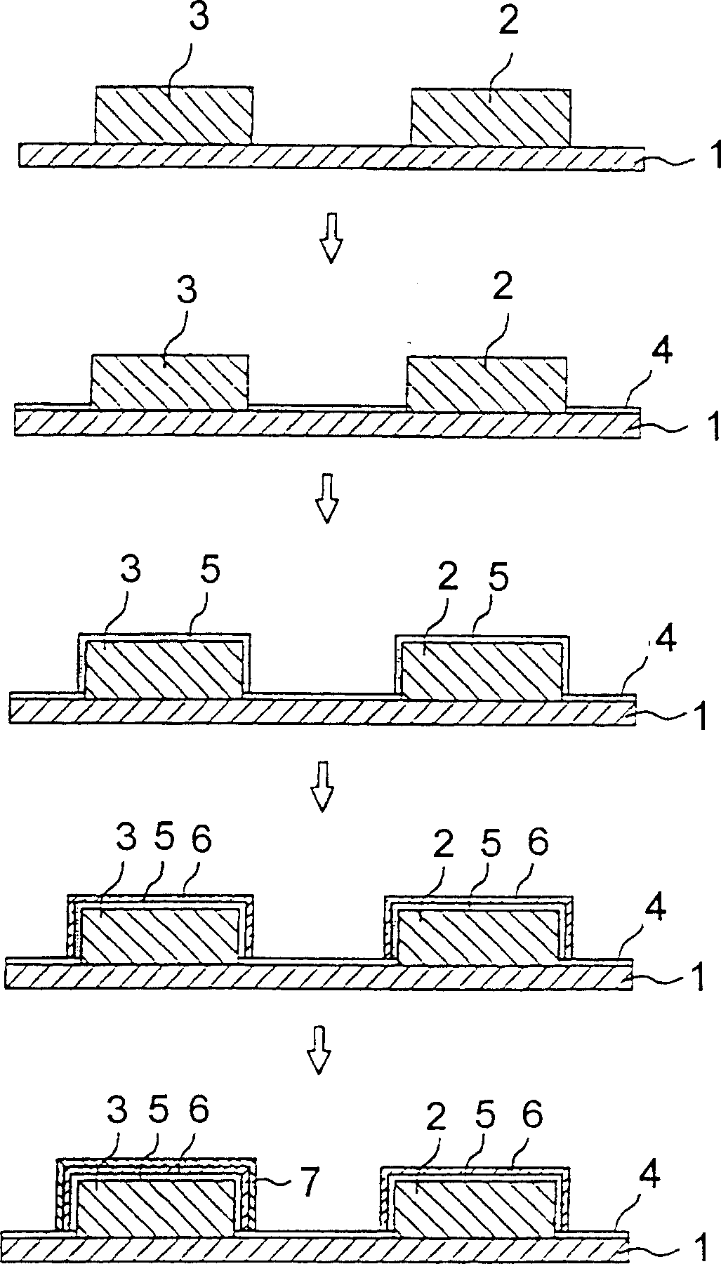
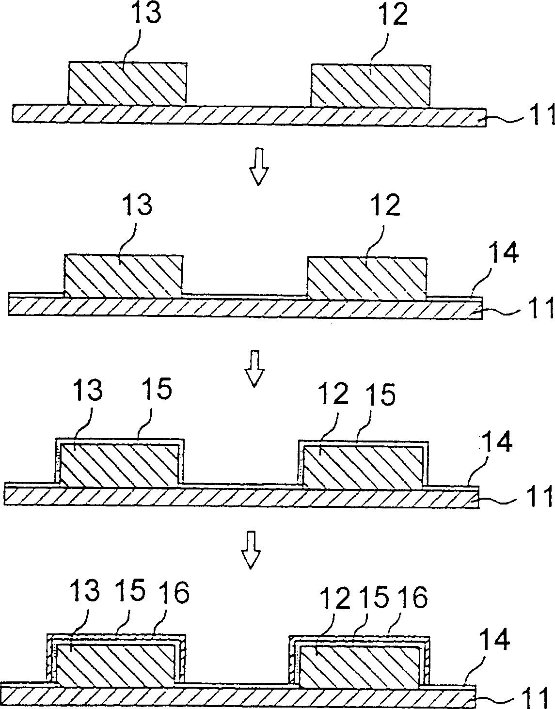
technical field [0001] The invention relates to a gold-silver alloy plating solution composition, which can be applied to the surface treatment of modular printed circuit boards (hereinafter referred to as modular PCBs) for component installation. More specifically, the present invention relates to a gold-silver alloy plating solution, by electroless nickel plating at the pad portion (pad portion) and the joint portion (tab portion) of the modular PCB, and then the nickel-plated surface of the modular PCB of nickel plating Immersed in a gold-silver alloy plating solution that forms an alloy coating containing 90-99% gold and 1-10% silver. Background technique [0002] In general, a modular PCB has a circuit pattern on a board, a land portion for electronic parts, and a connector portion electrically connected to an external device by a detachment and bonding method. Circuit patterns, land portions, and joint portions are usually made of copper. For this, figure 1 A top vi...

Claims


Application Information

Patent Timeline
Patent Type & Authority Patents(China)
IPC IPC(8): H05K3/24C25D3/62H05K1/09C23C18/16C23C18/48C23C18/52H05K3/18H05K3/40
CPCH05K3/244C23C18/48C23C18/16
Inventor 李炳虎杨德真安东基李哲敏郭兑圭许成龙全星郁申明彻全尚旭
Owner SAMSUNG ELECTRO MECHANICS CO LTD
Learn More