Process for preparing silicon melt from polysilicon charge

A technology of polysilicon and silicon melt, which is applied in the field of preparing silicon melt for growing monocrystalline silicon ingots and preparing molten silicon melt, which can solve the problems of increasing defects

Inactive Publication Date: 2000-12-06
MEMC ELECTONIC MATERIALS INC
View PDF4 Cites 24 Cited by
  • Summary
  • Abstract
  • Description
  • Claims
  • Application Information

AI Technical Summary

Problems solved by technology

However, this structure increases the chances of introducing defects in the growing crystal because there is more surface above the melt on which splashed silicon particles can accumulate and eventually fall back into the melt

Method used


Image

  • Process for preparing silicon melt from polysilicon charge
  • Process for preparing silicon melt from polysilicon charge
  • Process for preparing silicon melt from polysilicon charge

Examples


Embodiment Construction

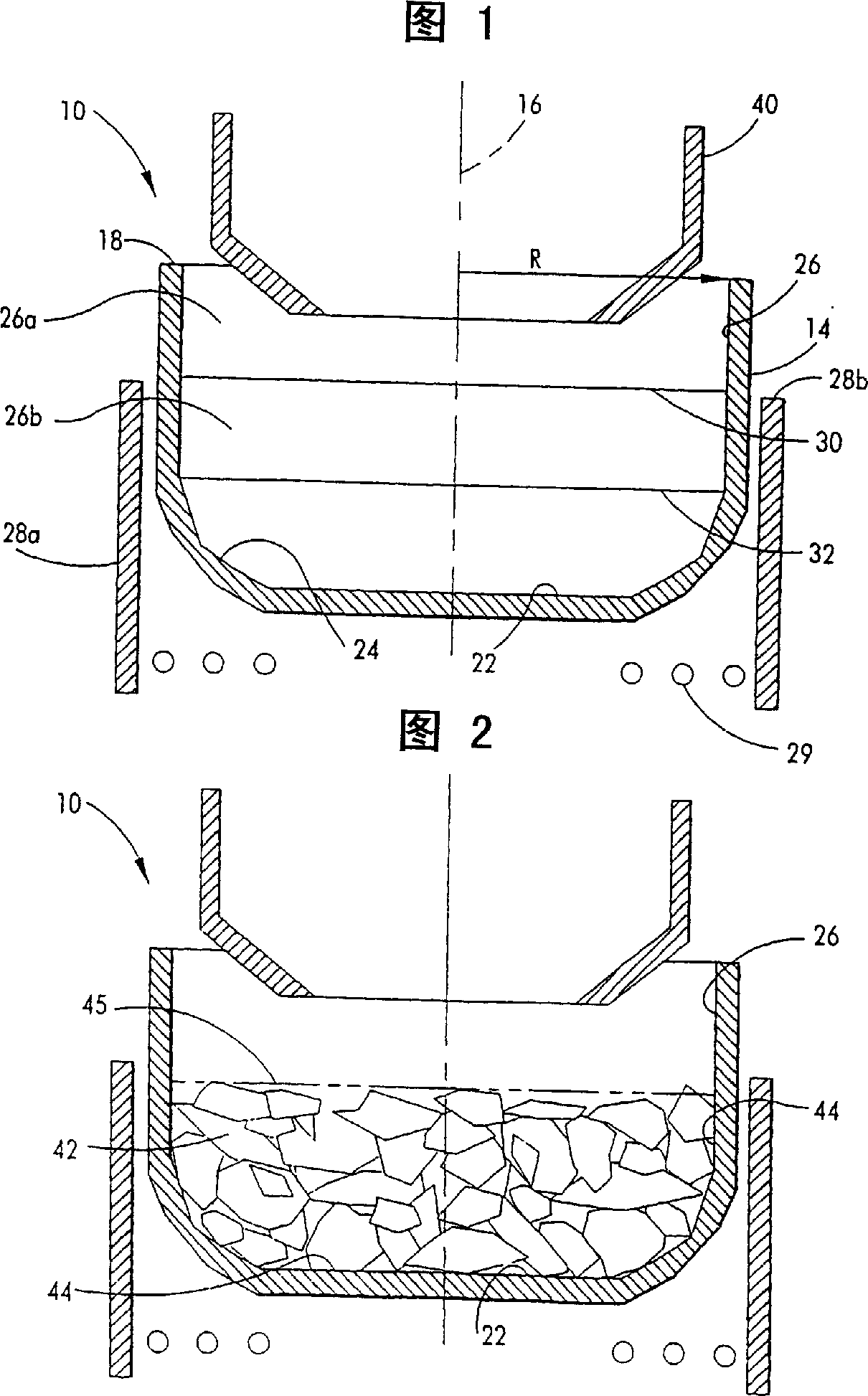
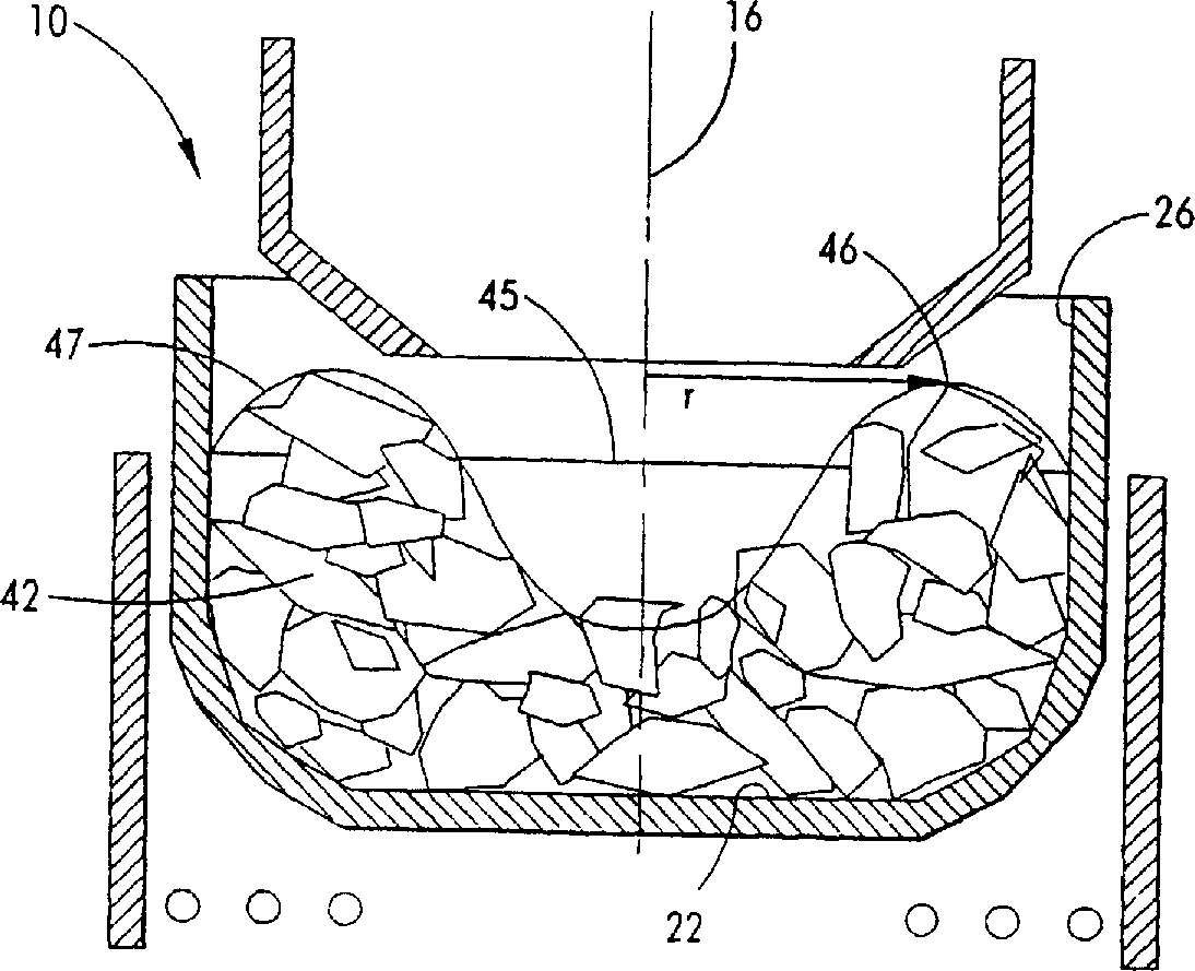
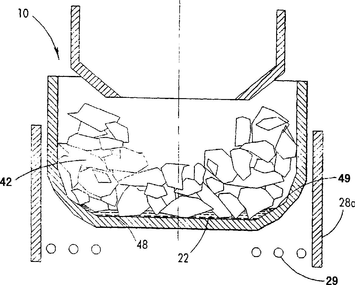
[0031]In accordance with the method of the present invention, chunk polycrystalline silicon is first charged into a Chowklarski crucible and melted to form a partially molten charge comprising both molten silicon and unmelted chunk silicon. Although the geometry of the crucible is not strictly specific, it should generally have inner and outer surfaces defining an at least partially open structure capable of containing or otherwise retaining a liquid, such as molten silicon. Referring now to FIG. 1 , an example silica crucible 10 generally has an inner surface 12 , an outer surface 14 , a centerline 16 and a top edge 18 . The inner surface 12 defines an open cavity for adding bulk polysilicon. Crucible 10 includes a bottom portion 22, corner portions 24 and side wall structures 26, hereinafter referred to as crucible bottom 22, corners 24 and side walls 26, respectively. The radius, R, of the crucible is measured radially outward from the centerline 16 to the inner surface of...


PUM


Abstract

A process for preparing a silicon melt from a polysilicon charge, for use in the production of single crystal silicon ingots by the Czochralski method, in a crucible which has a bottom, a sidewall formation, a centerline which is substantially parallel to the sidewall formation and which intersects a geometric centerpoint of the bottom, and a radius extending from the centerline to the sidewall formation. In the process, the crucible is loaded with chunk polysilicon to form a charge having a bowl-like shape, wherein initially the load generally slopes radially upwardly and outwardly from the centerline toward the sidewall formation to an apex and then slopes generally downwardly and outwardly from the apex to the sidewall formation. The bowl-shaped chunk polysilicon charge is heated to form a partially melted charge, and granular polysilicon is fed onto the partially melted charge to form a mixed charge of chunk and granular polysilicon. As the mixed charge is further heated to form a silicon melt, the unmelted chunk polysilicon present above the melt surface acts to deflect any molten silicon that may be splattered as granular polysilicon rapidly melts and hydrogen is released.

Description

Background of the invention [0001] The present invention generally relates to the preparation of monocrystalline silicon from molten silicon melt, and more particularly to a method for preparing molten silicon melt from a mixture of block and granular polysilicon, wherein the block polysilicon is first added to form a bowl, and Then add granular polysilicon. [0002] Most single crystal silicon used in the manufacture of microelectronic circuits is prepared using the Czochralski method ("CZ" method). In this method, a single crystal silicon ingot is produced by melting polycrystalline silicon (“polysilicon”) in a crucible, dipping a seed crystal into the molten silicon, and growing the seed crystal by pulling it up enough to obtain the desired diameter of the ingot. single crystal silicon of the desired diameter. [0003] The polysilicon that is melted to form a silicon melt is typically bulk polysilicon made by the Siemens process. Chunk polysilicon is generally irregular ...

Claims


Application Information

Patent Timeline
Patent Type & Authority Applications(China)
IPC IPC(8): C30B15/00C30B15/02C30B29/06
CPCC30B29/06C30B15/02
Inventor J·D·霍尔德
Owner MEMC ELECTONIC MATERIALS INC
Why Eureka
Try Eureka