Method for signal implant in making processing of mask type read-only memory

A read-only memory and manufacturing process technology, which is applied in semiconductor/solid-state device manufacturing, electrical components, circuits, etc., can solve the problems of limited device size, low yield, and easy peeling of photoresist masks, so as to increase output, Overcomes the effect of falling off easily

Active Publication Date: 2007-02-14
SEMICON MFG INT (SHANGHAI) CORP +1
View PDF3 Cites 0 Cited by
  • Summary
  • Abstract
  • Description
  • Claims
  • Application Information

AI Technical Summary

Problems solved by technology

[0004] The purpose of the present invention is to provide a new method of signal injection, so as to overcome the above-mentioned shortcomings such as photoresist mask easy to fall off, low yield, and limited device size.

Method used


Image

  • Method for signal implant in making processing of mask type read-only memory
  • Method for signal implant in making processing of mask type read-only memory
  • Method for signal implant in making processing of mask type read-only memory

Examples


Embodiment 1

[0029] Figure 1A-Figure 1I A particularly preferred embodiment of the invention is shown. In this embodiment, signal injection is performed using a tungsten hard mask.

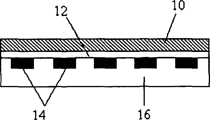
[0030] Such as Figure 1A As shown, after forming the MOS source region and the drain region and annealing, the p well (p well) 16 is located at the bottom of the substrate, the buried n+ (buried n-plus) 14 is located above the p well, and the gate oxide layer ( gate oxide) 12 is located above the p-well 16, and the gate 10 is located above the gate oxide layer 12.

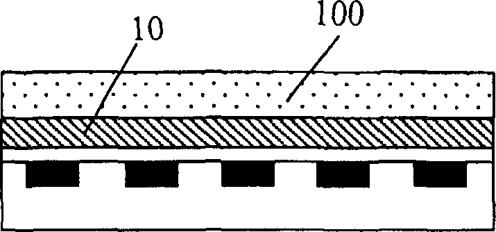
[0031] In the first step, a layer of SiO is deposited on the gate 10 2 100, such as Figure 1B shown. Here, SiO 2 The thickness of the layer 100 can be determined according to the magnitude of the signal injection energy and the material used for the mask, for example, about 600 Ȧ. Moreover, it is best for SiO 2 The layer is planarized, for example by chemical mechanical polishing, which is preferably used in the present invention.
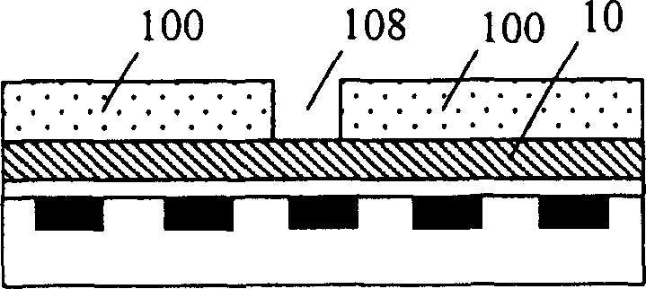
[00...

Embodiment 2

[0040] Figure 2A-Figure 2G A preferred embodiment of the invention is shown. In this example, using SiO 2 Hard mask for signal injection.

[0041] Such as Figure 2A As shown, after forming the MOS source and drain regions and annealing, the p well 16 is located at the bottom of the substrate, the buried n+14 is located above the p well, the gate oxide layer 12 is located above the p well 16, and the gate 10 is located on the gate oxide layer 12 .

[0042] In the first step, a layer of Si is deposited on the gate 10 3 N 4 120, such as Figure 2B shown. Here, Si 3 N 4 The thickness of the layer 120 can be determined according to the magnitude of signal injection energy and the material used for the mask, for example, about 2000 Ȧ. Moreover, it is best for Si 3 N 4Layer 120 is planarized, such as by chemical mechanical polishing, which is preferably employed in the present invention.

[0043] In the second step, use a pre-prepared mask to Si 3 N 4 Layer 120 is p...

Embodiment 3

[0049] Figure 3A-Figure 3G Another preferred embodiment of the invention is shown. In this example, using Si 3 N 4 Hard mask for signal injection. The step of embodiment three is basically the same as embodiment two, and its difference is: 140 is SiO 2 , 142 for Si 3 N 4 ; 148 is a hole pattern; 140 is etched using 10:1 HF.


PUM


Abstract

The invention discloses a method of implanting the signal in the preparation technique of the masking read-only memory. It chooses the hard materials as the masking and the hard materials are tungsten, silicon nitride and silicon dioxide. The method overcomes the disadvantage of the desquamating after the photolithography sol masking is developed, increases the yield and has benefit to reducing the size of the masking read-only memory to less than 0.13mum.

Description

technical field [0001] The present invention generally relates to the field of semiconductor device manufacturing, and more specifically, the present invention relates to a method for signal injection on a semiconductor substrate using a hard mask. Background technique [0002] Among various read-only memories, a mask-type read-only memory (Mask ROM) is a relatively simple one in structure and process. It uses the threshold voltage (threshold voltage) of the memory cell to represent the data value in it. When reading, the channel (channel) of the memory cell under a certain gate voltage is turned on and off to determine the data value, and the channel is opened. , Off is determined by the threshold voltage of the memory cell itself. [0003] In recent years, in the manufacturing process of the masked ROM, a method of signal injection (code implant) is widely used to adjust the threshold voltage to distinguish 0 / 1 signals. During signal implantation, for example, by ion imp...

Claims


Application Information

Patent Timeline
IPC IPC(8): H01L21/8246
Inventor 李文军陈军黄河
Owner SEMICON MFG INT (SHANGHAI) CORP
Why Eureka
Try Eureka