

Integrated circuit,method and apparatus for fine tuning clock signals of an integrated circuit
An integrated circuit, signal technology, applied in the direction of the phase angle between voltage and current, multiple input and output pulse circuits, electrical components, etc., can solve problems such as the inability of the chip to operate
- Summary
- Abstract
- Description
- Claims
- Application Information
AI Technical Summary
Problems solved by technology
Method used
Image

Examples
Embodiment Construction
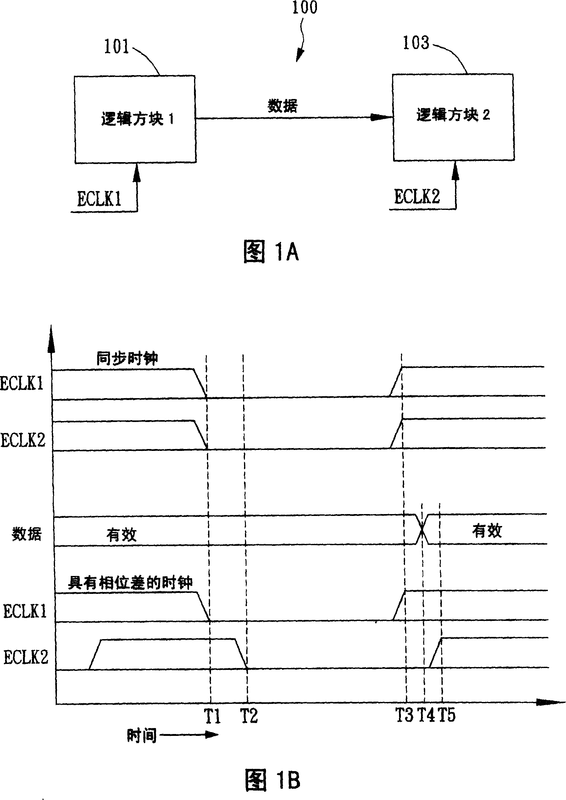
[0040] The following description is provided in the context of specific embodiments and prerequisites thereof to enable a person of ordinary skill in the art to utilize the invention. However, various modifications to the embodiments will be apparent to those skilled in the art, and the general principles discussed herein can also be applied to other embodiments. Thus, the present invention is not limited to the specific embodiments shown and described herein, but is to be accorded the widest scope consistent with the principles and novel features disclosed herein.
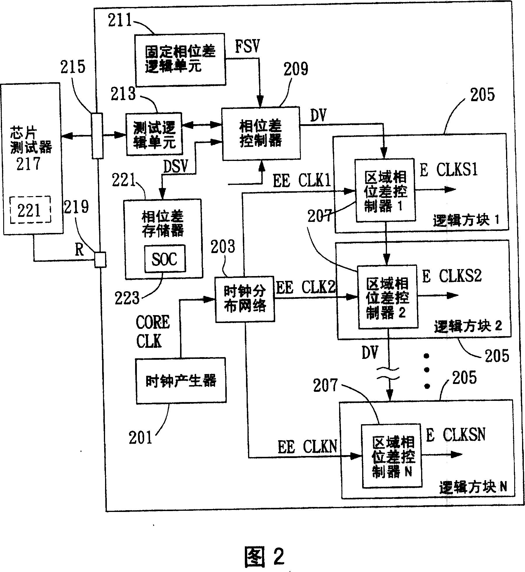
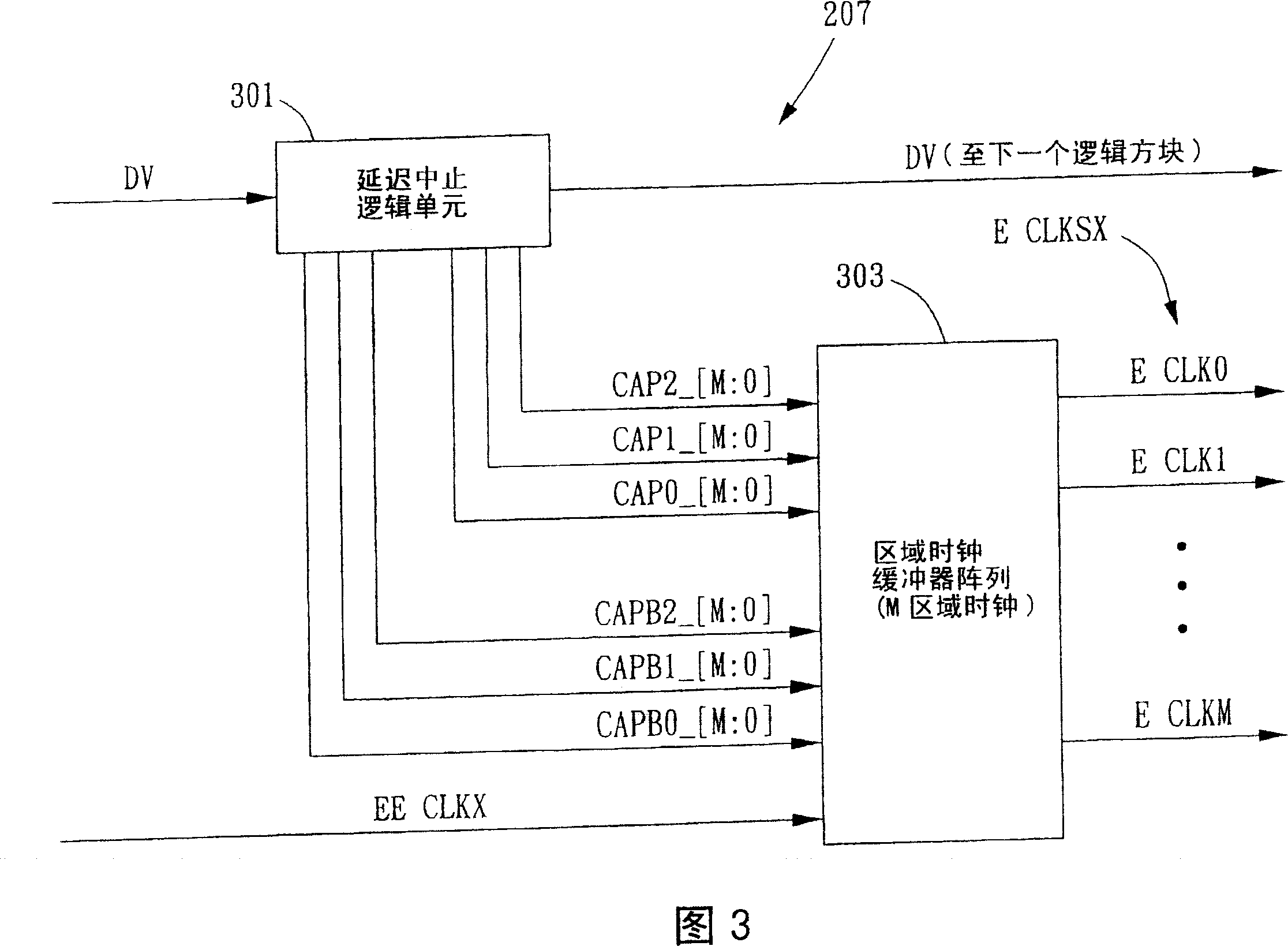
[0041] The present invention provides an integrated circuit (IC) designer with a device and method for dynamically controlling the regional clock and programming the optimal clock phase difference when testing and debugging an integrated circuit. into a composite element. Accordingly, the present invention develops a device and method for fine-tuning the integrated circuit clock signal on a combined component, wh...
PUM
 Abstract
Description
Claims
Application Information