Heterojunction field effect transistor

A heterojunction field effect and transistor technology, which is applied in the direction of transistors, semiconductor devices, electrical components, etc., can solve the problems of reduced current magnification, deterioration of transistor characteristics, and deterioration of n value, etc.

Inactive Publication Date: 2002-04-10
PANASONIC CORP
View PDF0 Cites 1 Cited by
  • Summary
  • Abstract
  • Description
  • Claims
  • Application Information

AI Technical Summary

Problems solved by technology

Figure 11(a) shows that if the recombination lifetime is small, it does not have much effect on the collector current, but the recombination current due to the base current is very large, causing n-value degradation
Moreover, Fig. 11(b) shows that if the recombination lifetime is small, the current amplification factor β is greatly reduced due to the increase in the recombination current of the base current as described above.
Therefore, the recombination life is short, which causes deterioration of transistor characteristics.

Method used


Image

  • Heterojunction field effect transistor
  • Heterojunction field effect transistor
  • Heterojunction field effect transistor

Examples


no. 1 Embodiment

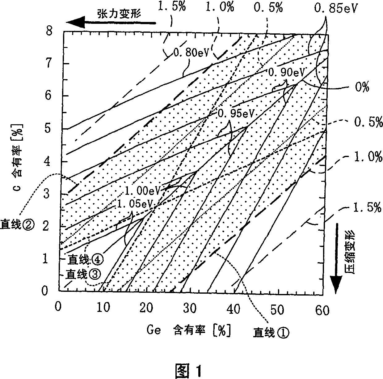
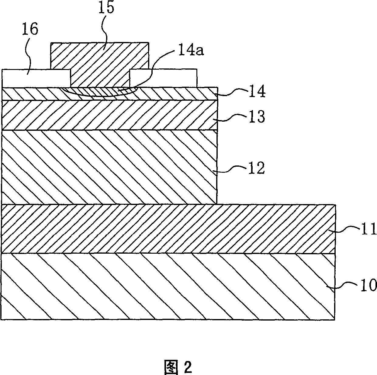
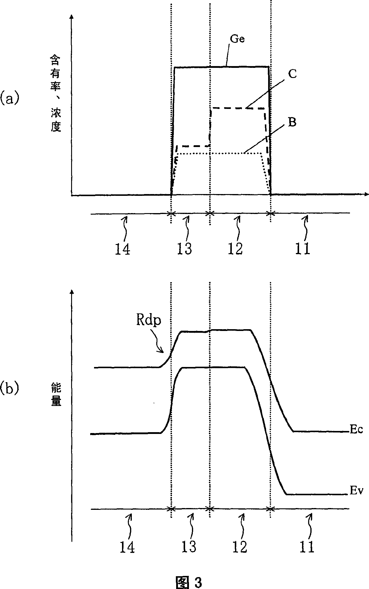
[0059] 3(a) and (b) show the C and Ge contents of the first base region and the second base region and the concentration of impurity boron (B) in the first embodiment, and the emitter region when a voltage is applied. - Energy band diagram of base region-collector region. In addition, illustration of the concentration of n-type impurities is omitted in FIG. 3( a ).

[0060] As shown in FIG. 3( a ), in this embodiment, the Ge content rate is set to a constant value (for example, 26.8%) throughout the first base region 12 and the second base region 13 . On the other hand, the content of C was 0.91% in the first base region 12 and 0.35% in the second base region 13 . That is, the first base region 12 is made of SiGe 0.268 C 0.0091 layers, the second base region 13 is made of SiGe 0.268 C 0.0035 layer composition.

[0061] At this time, SiGe 0.268 C 0.0091 The bandgap of the layer is about 0.95eV, SiGe 0.268 C 0.0035 The bandgap of the layer is about 0.92eV. Therefore, ...

no. 2 Embodiment

[0066] 4(a) and (b) show the C and Ge contents of the first base region and the second base region and the concentration of impurity boron (B) in the second embodiment, and the emitter region when a voltage is applied. - Energy band diagram of base region-collector region. In addition, illustration of the concentration of n-type impurities is omitted in FIG. 4( a ).

[0067] The present embodiment is characterized in that the band gaps of the two regions 12 and 13 are made equal by adjusting the Ge and C contents in the first base region 12 and the second base region 13 . Therefore, the Ge content rate is not set to the same value in the first and second base regions, but the Ge content rate in the first base region 12 is set higher than the Ge content rate in the second base region 13 That's it. When the composition in the SiGeC layer is represented by the general formula Si 1-x-y Ge x C y When the difference in the C content of the first base region 12 and the second ba...

no. 3 Embodiment

[0072] 5(a) and (b) show the C and Ge contents of the first base region and the second base region and the concentration of impurity boron (B) in the third embodiment, and the emitter region when a voltage is applied. - Energy band diagram of base region-collector region. In addition, illustration of the concentration of n-type impurities is omitted in FIG. 5( a ).

[0073] In this embodiment, it is characterized in that by adjusting the content ratios of Ge and C in the first base region 12 and the second base region 13, the boundary between the first base region 12 and the second base region 13 is made The band gaps of the two are equal, so that the band gap of the first base region 12 changes toward the direction of accelerating base transition electrons. For this reason, when the composition in the SiGeC layer is represented by the general formula Si 1-x-y Ge x C y Indicates that when the difference in C content between the end of the first base region 12 on the second...


PUM


Abstract

A hetero bipolar transistor is provided to have characteristics such as high current amplification factor or the like by suppressing the recombination current of the emitter and base while lowering the drive voltage. An Si-collector buried layer(11), the first base region(12) mode of the SiGeC layer having a high C content, the second base region(13) made of the SiGeC layer or an SiGe layer having a low C content, and an Si-cap layer(14) having an emitter region(14a), are laminated on an Si substrate(10). The C content of at least an emitter region side end of the second base region is less than 0.8%. Thus, in a depletion layer of an emitter-base junction, formation of the recombination center of the C is suppressed. An improvement in electrical characteristic such as a current amplification factor or the like due to a reduction in the recombination current is realized while maintaining low voltage drive properties.

Description

technical field [0001] The present invention relates to a heterojunction field effect transistor using a semiconductor layer including silicon, and more particularly to a measure for lowering the driving voltage. Background technique [0002] In the past, as a high-performance device, the composition of the emitter region and the base region was changed in order to make the bandgap of the emitter region larger than that of the base region, thereby greatly improving the injection efficiency of the emitter, thereby improving the transistor characteristics. Heterojunction Field Effect Transistor (hereinafter referred to as HBT) has attracted much attention. Such HBTs are increasingly being used as devices in the microwave and millimeter wave frequency domains, particularly because of their excellent high-frequency characteristics. In the past, HBTs were mostly made of a combination of GaAs and AlGaAs, which are group III-V compound semiconductors. However, in recent years, the...

Claims


Application Information

Patent Timeline
Patent Type & Authority Applications(China)
IPC IPC(8): H01L29/737
CPCH01L29/7378H01L29/737
Inventor 丰田健治幸康一郎高木刚大西照人久保实
Owner PANASONIC CORP
Why Eureka
Try Eureka