Monocrystalline silicon wafer crystal orientation calibrating method

A silicon wafer and crystal orientation technology, which is applied in the field of calibration of single crystal silicon wafer crystal orientation, can solve problems such as product performance degradation, device failure, and failure to meet the processing requirements of silicon micro devices, etc., to reduce processing errors, improve accuracy, The effect of eliminating machining errors

Inactive Publication Date: 2002-04-17
XI AN JIAOTONG UNIV
View PDF0 Cites 4 Cited by
  • Summary
  • Abstract
  • Description
  • Claims
  • Application Information

AI Technical Summary

Problems solved by technology

However, since most of the wafers used in actual production are general-purpose products in the IC industry, the positioning accuracy of the crystal orientation gap is only ±1-2°, which is far from meeting the processing requirements of silicon micro devices. Therefore, in some micro During t

Method used


Image

  • Monocrystalline silicon wafer crystal orientation calibrating method

Examples


Embodiment 1

[0021] Embodiment 1: see accompanying drawing.

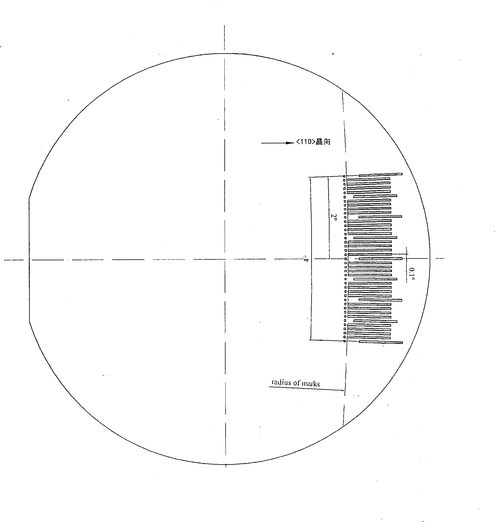
[0022] According to the size of the wafer and the requirements of processing accuracy, the layout for crystal orientation calibration is designed, and the corresponding mask is processed by conventional technology. The layout design of the mask is shown in the attached drawing. The comparison pattern of the layout consists of a A group of rectangular strips distributed in a fan shape, the centers of these rectangular strips are located on the center of a great circle, the angle between two adjacent rectangular strips is 0.05°, and all these rectangular strips are distributed at an angle of 2 ° and within the fan-shaped area with the large crystal direction of the wafer as the angle bisector, and with the large crystal direction of the silicon wafer as the axis of symmetry, these rectangular strips are symmetrically distributed; then a masking layer is processed on the silicon wafer, using the mask Plate, transfer the comparison ...

Embodiment 2

[0024] According to the size of the wafer and the requirements of processing accuracy, the layout used for crystal orientation calibration is designed, and the corresponding mask plate is processed by conventional technology. The layout design of the mask plate refers to the attached drawing. A group of rectangular strips distributed in a fan shape. The centers of these rectangular strips are located on the center of a great circle, and their long sides are parallel to the radial direction of the great circle. The angle between two adjacent rectangular strips is 0.1°. All These rectangular strips are distributed in a fan-shaped area with an included angle of 4° and the major crystal orientation of the wafer as the bisector of the angle. Taking the major crystal orientation of the silicon wafer as the axis of symmetry, these rectangular strips are symmetrically distributed. Then a masking layer is processed on the silicon wafer, and the comparison pattern is transferred to the m...


PUM


Abstract

The invention relates to a method to calibrate crystal orientation of mono-crystalline silicon wafer used in area of micro mechanism and microelectronics. The crystal orientation of wafer is clearly exposed by means of claborate reference patterns and following pre-etching process. The error calibrating the crystal orientation of wafer is controlled within plus or minus 0.1 degree, by observing the etching results formed from different reference patterns. With the etching results being processed further by using digital image processing technique, the calibrating accuracy can be improved to plus or minus 0.05 degree or even higher.

Description

1. Technical field [0001] The invention belongs to the technical field of micromechanics and microelectronics, in particular to a method for marking the crystal orientation of a single crystal silicon wafer. 2. Background technology [0002] At present, using the anisotropic etching characteristics of single crystal silicon materials, wet chemical etching processes are used to form structures of various shapes, which is one of the main processing methods for micro-devices. In this processing technology, the alignment accuracy of the pattern on the mask plate and the large crystal direction of the wafer has a decisive impact on the manufacturing accuracy of the micro-device to be processed. Therefore, it is necessary to ensure the orientation of the mask plate during the pattern transfer process. Being able to accurately locate on the specified crystal orientation is a key technology for processing qualified micro devices. However, since most of the wafers used in actual pro...

Claims


Application Information

Patent Timeline
IPC IPC(8): G03F1/80G03F7/00H01L21/027H01L21/66
Inventor 贾陈平屈梁生
Owner XI AN JIAOTONG UNIV
Why Eureka
Try Eureka