

Thin film transistor array and its manufacturing method and display board using same
A technology of thin film transistor and manufacturing method, applied in the field of TFT array, can solve problems such as poor characteristics, and achieve the effects of simplified manufacturing process and high pixel numerical aperture
- Summary
- Abstract
- Description
- Claims
- Application Information
AI Technical Summary
Problems solved by technology
Method used
Image

Examples
Embodiment 1
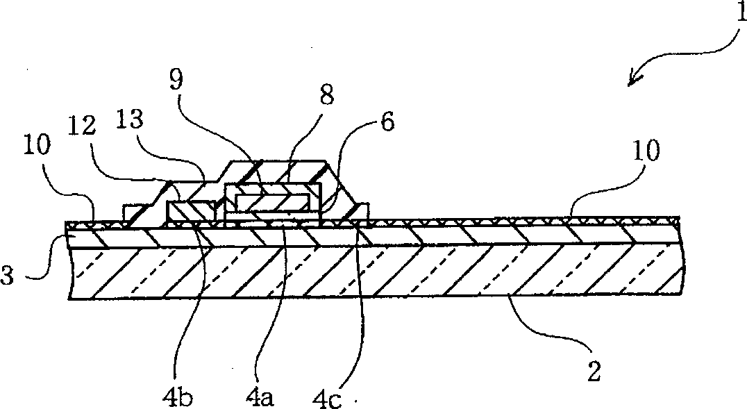
[0119] In this embodiment, a TFT array using a so-called top-gate TFT in which a gate electrode of a TFT is arranged in an upper layer than a channel portion will be described.
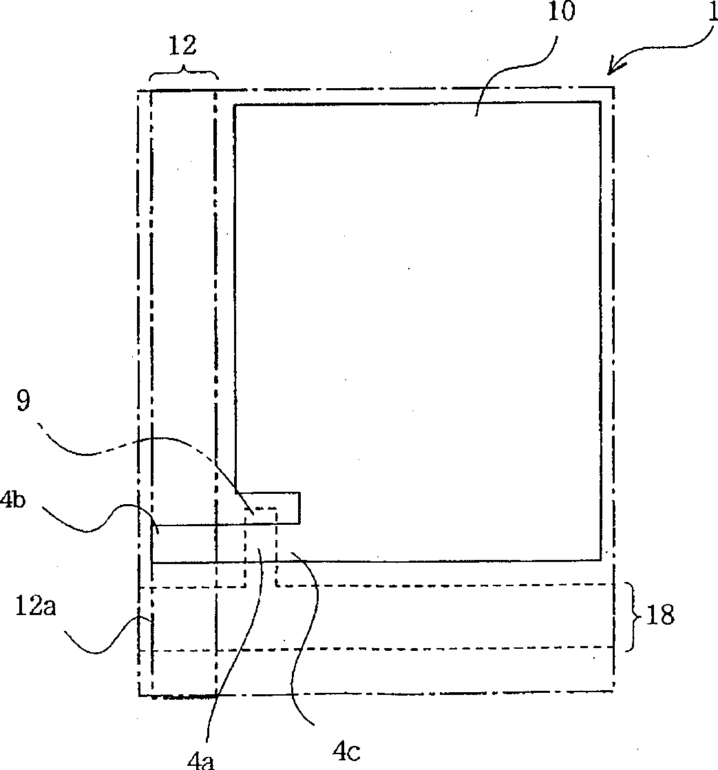
[0120] exist Figure 1a as well as Figure 1b The TFT array of this embodiment is shown in . As shown in the figure, the pixel electrode 10 is disposed on the same layer as the channel portion 4a, the source portion 4b, and the drain portion 4c which are semiconductor layers of the TFT, and is integrally formed with them. The pixel electrode 10, the channel portion 4a, the source portion 4b, and the drain portion 4c are made of a semiconductor material imparted with conductivity.
[0121] The TFT array of this example is produced, for example, as follows.
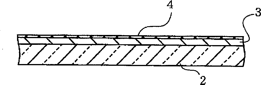
[0122] Such as Figure 2a As shown, on the surface of the cleaned transparent glass substrate 2, a film composed of silicon oxide with a thickness of 0.4 μm is formed as an undercoat layer (protective film) 3 by chemical vapor deposition (CVD), ...
Embodiment 2
[0153] In this embodiment, a TFT array using so-called bottom-gate TFTs in which the gate electrodes of TFTs are arranged in the lower layer of the channel portion will be described.
[0154] The TFT array of this embodiment is shown in Figure 9 middle. As shown in the figure, the pixel electrode 10 is arranged on the same layer as a channel portion 23a, a source portion 23b, and a drain portion 23c which are semiconductor layers of a TFT, and is integrally formed with them. The pixel electrode 10, the channel portion 23a, the source portion 23b, and the drain portion 23c are made of a semiconductor material imparted with conductivity.
[0155] The TFT array of this example is produced, for example, as follows.
[0156] Such as Figure 10a As shown, on the surface of the cleaned transparent glass substrate 2, a film composed of silicon oxide with a thickness of 0.4 μm as an undercoat layer 3 is formed by chemical vapor deposition (CVD), and then by sputtering , a metal la...
Embodiment 3
[0170] In this embodiment, an example of a TFT array using a semiconductor material film also as an insulating element will be described.
[0171] exist Figure 11a as well as Figure 11b The TFT array of this embodiment is shown above. In this embodiment, without processing its shape, the semiconductor material film is separated into each element function of the TFT array. In addition, main elements of the gate signal line 18, the gate electrode 9, and the source signal line 12 are formed by processing the same layer. Therefore, the manufacturing process of the TFT array is further simplified compared with the above-mentioned embodiments.
[0172] The TFT array of this example is produced, for example, as follows.
[0173] Such as Figure 12a As shown, on the cleaned transparent glass substrate 2, a film composed of silicon oxide with a thickness of 0.4 μm as an undercoat layer 3 is formed by chemical vapor deposition (CVD), and then on the undercoat layer 3 , by sputte...
PUM
| Property | Measurement | Unit |
|---|---|---|
| thickness | aaaaa | aaaaa |
| thickness | aaaaa | aaaaa |
| thickness | aaaaa | aaaaa |
Abstract
Description
Claims
Application Information