Polysilicon film transistor of liquid crystal display device and its mfg. method

A polysilicon, intermediate layer technology, applied in transistors, semiconductor/solid-state device manufacturing, instruments, etc., can solve the problems of increased production cost and process deviation, and achieve the effect of simplifying the manufacturing method and preventing surface damage

Inactive Publication Date: 2002-12-04
SAMSUNG DISPLAY CO LTD
View PDF0 Cites 23 Cited by
  • Summary
  • Abstract
  • Description
  • Claims
  • Application Information

AI Technical Summary

Problems solved by technology

[0021] The more the number of lithography processes increases, the more the possibility of production cost and process deviation increases

Method used


Image

  • Polysilicon film transistor of liquid crystal display device and its mfg. method
  • Polysilicon film transistor of liquid crystal display device and its mfg. method
  • Polysilicon film transistor of liquid crystal display device and its mfg. method

Examples


Embodiment 1

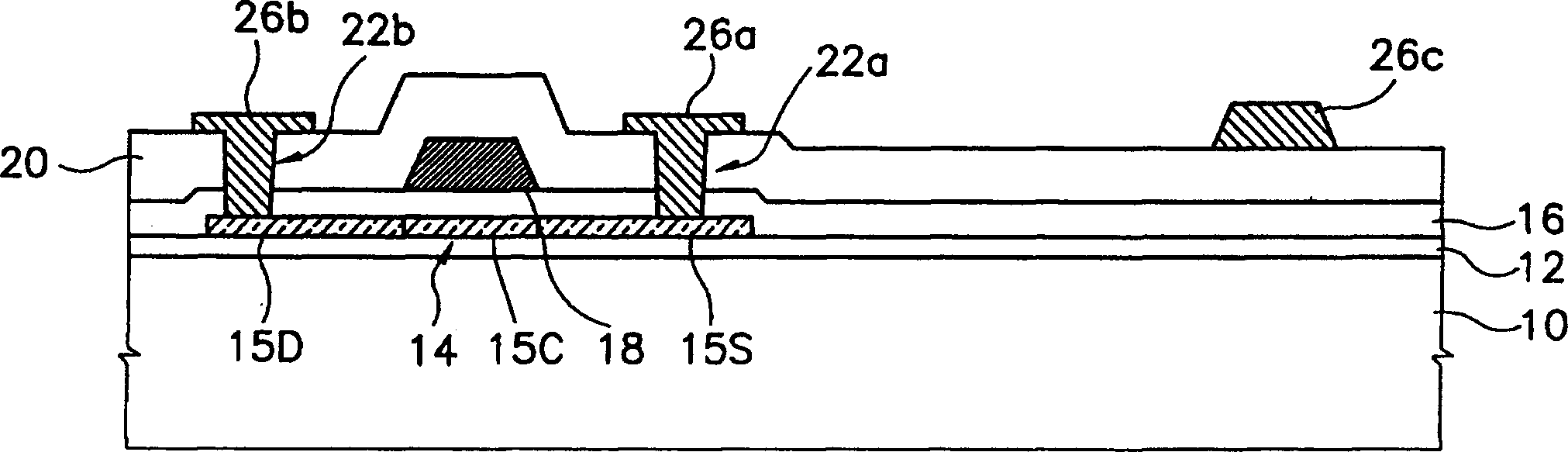
[0053] figure 2 A cross-sectional view of a polysilicon TFT according to a first embodiment of the present invention is shown.

[0054] refer to figure 2 , on a transparent substrate 100 made of a transparent insulating material such as glass, quartz or sapphire, a barrier layer 102 is formed. A polysilicon effective pattern 104 is formed on the barrier layer 102 . The effective pattern 104 includes a lower electrode 105T integrally formed with the effective pattern.

[0055] On the effective pattern 104 and the barrier layer 102, a gate insulating layer 106 made of silicon nitride or silicon oxide is formed. A gate electrode 108a is formed on the gate insulating layer 106 across the effective pattern 104 to define source / gate regions 105S and 105D. That is, a part of the effective pattern 104 overlapped by the gate electrode 108a is used as the channel region 105C of the TFT, and one side of the effective pattern 104 divided with respect to the channel region 105C locat...

Embodiment 2

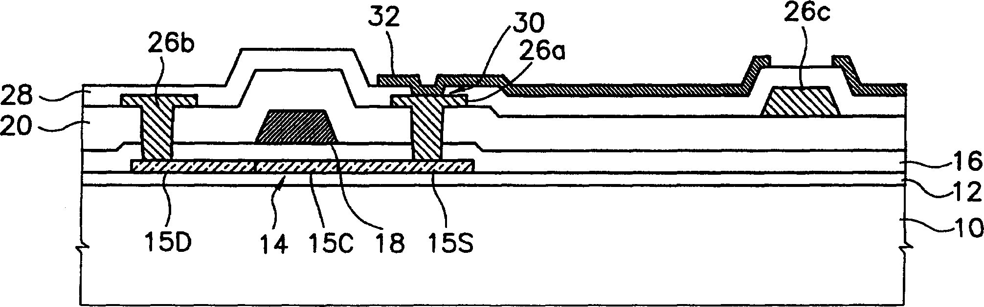
[0081] Figure 6 A cross-sectional view of a polysilicon TFT according to a second embodiment of the present invention is shown.

[0082] refer to Figure 6 , after forming the data line 114a, the pixel electrode 114b and the conductive pattern 114c (using the fifth mask) for connecting the gate pad in the same manner as in Embodiment 1, such as silicon nitride (SiN x ) is deposited on the entire surface of the synthetic material to form a passivation layer 116 . Then, the passivation layer 116 on the conductive pattern 114c is etched using a photolithography process to expose the conductive pattern 114c (using a sixth mask).

[0083] If the passivation layer is formed as described above, compared with Embodiment 1, the number of masks is increased to six. However, it is advantageous to prevent the data line 114a and the pixel electrode 114b from being contaminated, and to protect the patterning. Preferably, the passivation layer 116 has a desired thickness so that an elec...

Embodiment 3

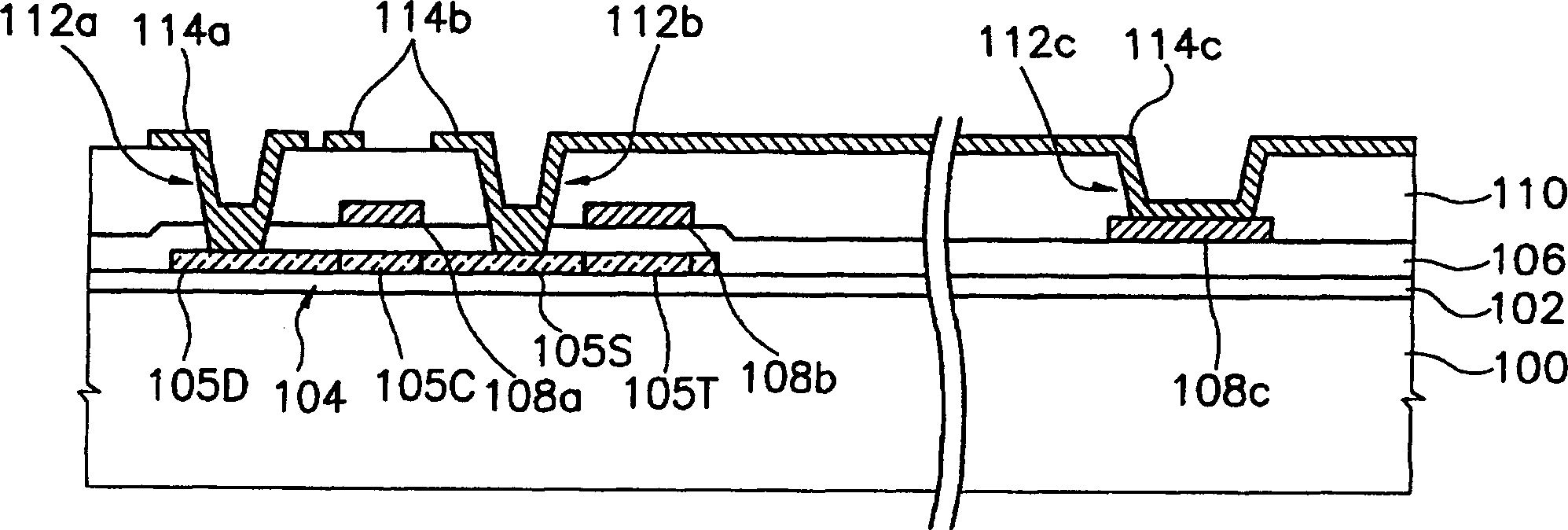
[0085] Figure 7A to Figure 7D is a cross-sectional view illustrating a method of manufacturing a polysilicon TFT according to a third embodiment of the present invention.

[0086] refer to Figure 7A , on the transparent substrate 100, in a manner similar to that in Embodiment 1, a barrier layer 102, an effective pattern 104, a gate insulating layer 106, gate lines and capacitor lines 108b are formed. The gate line includes a gate line formed in the display area, a gate electrode 108a as a part of the gate line, and a gate pad 108c formed in a pad area located outside the display area. During the formation of the gate lines, signal transmission lines (not shown) spaced a predetermined distance away from the gate lines and extending in a direction perpendicular to the gate lines are also formed together with the gate lines.

[0087] Then, an organic insulating material is deposited to a thickness of several thousand Å on the gate line, the capacitor wire 108 b and the gate i...


PUM


Abstract

The invention discloses a polysilicon TFT used for LCD and a manufacturing method thereof. The TFT includes an effective pattern formed on the substrate, a gate insulating layer formed on the substrate including the effective pattern, and a gate insulating layer formed on the gate insulating layer across the effective pattern and includes a method for defining the first impurity region, the second impurity region and the The gate line of the gate electrode of the channel region, the insulating interlayer formed on the gate insulating layer including the gate line, the data line formed on the insulating interlayer and connected to the second impurity region through the first contact hole, and formed on the The pixel electrode on the same insulating interlayer as the data line and connected to the first impurity region through the second contact hole, wherein the first contact hole is formed on the second impurity region through the gate insulating layer and the insulating interlayer, and the second contact A hole is formed on the first impurity region through the gate insulating layer and the insulating interlayer. The number of masks can be reduced to 5 or 6, thus simplifying the production process.

Description

technical field [0001] The present invention relates to a thin film transistor and a manufacturing method thereof, and more particularly, to a polysilicon thin film transistor having a p-type sum transistor to form a CMOS (compensated metal oxide semiconductor) structure for a driving circuit for an LCD (liquid crystal display), and methods of manufacture thereof. Background technique [0002] In today's information-oriented society, the role of electronic displays is becoming more and more important. All kinds of electronic displays are widely used in various industrial fields. [0003] In general, an electronic display is a device used to convey information to the human eye. That is, electrical information signal outputs from various electronic devices are converted into visually discernible optical information signals in an electronic display. Thus, electronic displays serve as a bridge connecting people and electronic devices. [0004] Elect...

Claims


Application Information

Patent Timeline
Patent Type & Authority Applications(China)
IPC IPC(8): H01L29/786G02F1/1362G02F1/1368G09F9/30G09F9/35H01L21/77H01L21/84H01L27/12
CPCG02F1/136227H01L27/1214H01L27/1288G02F1/136236H01L29/786
Inventor 黄长元郑宇席朴泰炯金县裁文奎善姜淑映
Owner SAMSUNG DISPLAY CO LTD
Why Eureka
Try Eureka