Method for decreasing disc defect in chemicomechanical copper grinding

A chemical mechanical, dishing technology, applied in chemical instruments and methods, other chemical processes, electrical components, etc., to solve problems such as unevenness

Inactive Publication Date: 2003-02-19
UNITED MICROELECTRONICS CORP
View PDF0 Cites 6 Cited by
  • Summary
  • Abstract
  • Description
  • Claims
  • Application Information

AI Technical Summary

Problems solved by technology

The unevenness caused by dishing is due to the different polishing rates of different materials

Method used


Image

  • Method for decreasing disc defect in chemicomechanical copper grinding
  • Method for decreasing disc defect in chemicomechanical copper grinding
  • Method for decreasing disc defect in chemicomechanical copper grinding

Examples


Embodiment Construction

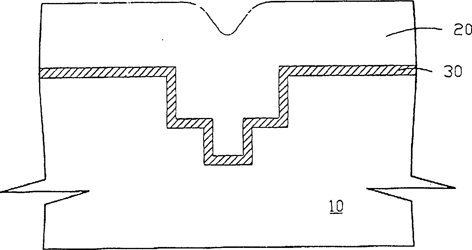
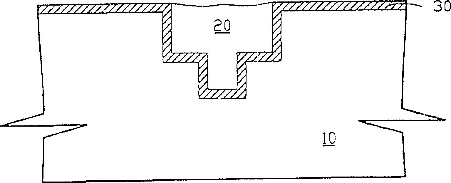
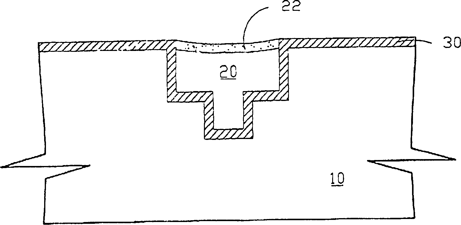
[0011] The semiconductor design of the present invention can be widely applied in many semiconductor designs, and can utilize many different semiconductor materials to make, when the present invention illustrates the method of the present invention with a preferred embodiment, those who are familiar with this field should have It is recognized that many steps can be changed, and materials and impurities can also be replaced, and these general replacements undoubtedly do not depart from the spirit and scope of the present invention.

[0012] Secondly, the present invention is described in detail with schematic diagrams as follows. When describing the embodiments of the present invention in detail, the cross-sectional view showing the semiconductor structure will not be partially enlarged according to the general scale in the semiconductor manufacturing process for the convenience of explanation, but it should not be used as a limited definition. Know. In addition, in actual pro...


PUM


Abstract

This invention provides a reducing conductance structure dishing and erosion method in chemical mechanical grinding containing at least a dielectric layer with at least a dielectric window hole; forming a barrier layer on dielectric layer and the window hole; forming a conductive layer such as a copper layer on the barrier layer to fill in the dielectric window hole to form a conductive structure and removing part of conductive layer to expose part of the barrier layer to be polished as well as the conductive structure. With a reacted reagent so as to form a metal compound on the conductive structure prevented from dishing or erosion.

Description

(1) Technical field [0001] The present invention relates to a method for manufacturing semiconductor integrated components, in particular to a method for planarizing conductive copper wires and internal connections using a chemical mechanical process. (2) Background technology [0002] As the overall size of integrated circuits shrinks, the performance of internal components tends to be mixed, which is a natural characterization of semiconductor physics; that is, the speed and functional capabilities of components will increase simultaneously. In any case, the speed of the entire circuit is more dependent on the delay speed of the signal on the interconnection lines connecting the internal components. With the advent of extremely large and ultra-large integrated circuits, it is more and more important to form the internal connection conductors between components and the metal conductors between circuits in semiconductors to have high signal transmission and low resistance va...

Claims


Application Information

Patent Timeline
IPC IPC(8): H01L21/321H01L21/768
CPCH01L21/7684H01L21/3212H01L21/76886
Inventor 许嘉麟余志展胡绍中蔡腾群
Owner UNITED MICROELECTRONICS CORP
Why Eureka
Try Eureka