Semiconductor storage device

A storage device, semiconductor technology, applied in the direction of static memory, read-only memory, digital memory information, etc., can solve problems such as circuit failure, power supply voltage fluctuation, sense amplifier failure, etc., achieve stable operation, stable power supply voltage, and prevent failure Effect

Inactive Publication Date: 2003-09-24
FUJITSU LTD
View PDF1 Cites 6 Cited by
  • Summary
  • Abstract
  • Description
  • Claims
  • Application Information

AI Technical Summary

Problems solved by technology

Therefore, there is noise caused by the drop or rise of the power supply voltage due to the spike current at the time of the data read operation in the conventional ferroelectric memory device
[0017] In addition, fluctuations in the power supply voltage occur when the sense amplifier starts to activate, which amplifies a small potential difference, and there is a problem that the sense amplifier may malfunction
In addition, the power supply voltage outside the memory chip may be affected by fluctuations in the power supply voltage of the internal circuits of the memory chip, and may cause failure of other circuits on the system including the memory chip such as an IC card

Method used


Image

  • Semiconductor storage device
  • Semiconductor storage device
  • Semiconductor storage device

Examples


Embodiment Construction

[0040] A description will now be given of preferred embodiments of the present invention with reference to the accompanying drawings.

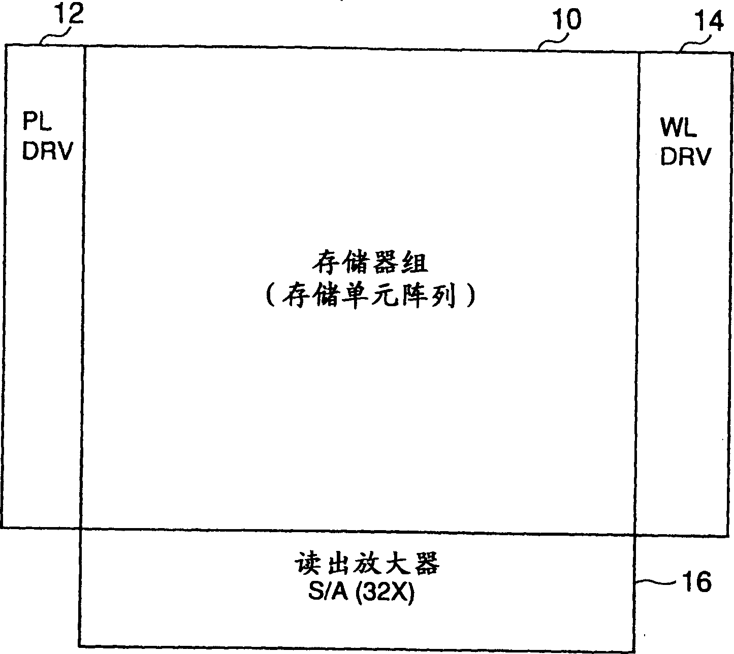
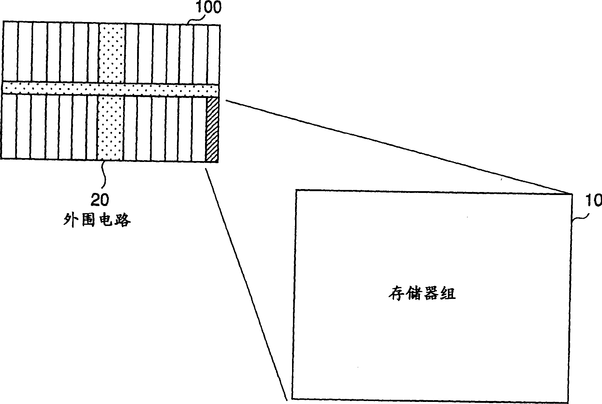
[0041] Figure 4A and 4B A basic configuration of a memory block of the semiconductor memory device in the first preferred embodiment of the present invention is shown.

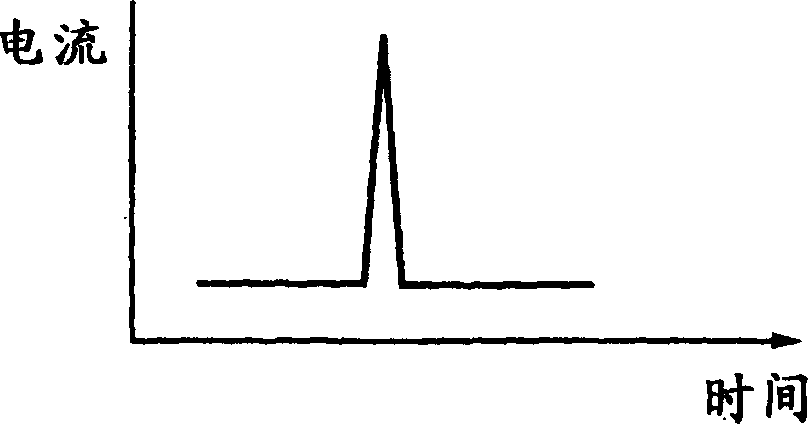
[0042] The semiconductor memory device of the present invention is applied to a ferroelectric memory device using a ferroelectric memory as a memory element. Figure 4A The semiconductor memory device of the present invention is capable of reducing peak current in data read / write operations by reducing the number of sense amplifiers that simultaneously start operating in the same memory bank.

[0043] To achieve this, the memory group divided by each word line is divided into a plurality of memory blocks. In this embodiment, two memory blocks are provided: memory block-1 and memory block-2. By separately providing a sense amplifier control circuit 16-1 for controlling the...


PUM


Abstract

A semiconductor memory device including a memory group divided into a plurality of memory blocks including a first memory block and a second memory block. The first sense amplifier control unit activates the sense amplifier connected to the first memory block in response to the first activation signal. The second sense amplifier control unit activates the sense amplifier connected to the second memory block in response to the second activation signal. The signal control unit outputs the first activation signal and the second activation signal to the first sense amplifier control unit and the second sense amplifier control unit which are separated from each other, and the signal control unit makes the first sense amplifier control unit and the second sense amplifier control unit separate after outputting the first activation signal. The activation signal is delayed by a predetermined time to output the second activation signal to the second sense amplifier control unit.

Description

[0001] This application is based on and claims Japanese Patent Application No. 2002-069065 filed on March 13, 2002, the entire contents of which are hereby incorporated by reference. technical field [0002] The present invention generally relates to a semiconductor memory device including a plurality of memory banks, and more particularly to a nonvolatile semiconductor memory which reduces consumption current at the time of operation of each memory bank to stabilize reading or writing of the semiconductor memory device Enter operation. Background technique [0003] In recent years, the information society has rapidly developed, and large-scale storage devices have required information processing devices such as multipurpose IC cards that pack various application programs. In addition, the use of non-contact type IC cards is increasing, and power supplied to the IC cards is obtained by using microwaves as signal carriers of data to be transmitted. Therefore, there is a need...

Claims


Application Information

Patent Timeline
Patent Type & Authority Applications(China)
IPC IPC(8): G11C11/22G11C7/06G11C7/18G11C8/12
CPCG11C7/06G11C7/18G11C8/12G11C2207/065G11C16/32G11C11/2293
Inventor 铃木英明中岛雅夫
Owner FUJITSU LTD
Why Eureka
Try Eureka