Electronic device

A technology for electronic devices and electronic components, applied in the directions of tin feeding devices, circuits, assembling printed circuits with electrical components, etc., can solve the problems such as the absence of low-temperature end solder, use restrictions, and damage to Si chips.

Inactive Publication Date: 2003-09-24
RENESAS ELECTRONICS CORP
View PDF0 Cites 18 Cited by
  • Summary
  • Abstract
  • Description
  • Claims
  • Application Information

AI Technical Summary

Problems solved by technology

However, there is no high-reliability low-temperature-side solder that can bond without melting the Sn-5Sb solder, taking into account things such as temperature irregularities in the substrate in the reflow furnace.
On the other hand, although Au-20Sn solder (melting point: 280 degrees Celsius) is regarded as a high-temperature solder, its use is limited due to its hard material and high cost
In particular, this solder cannot be used when bonding an Si chip to a material having a coefficient of expansion greatly different from that of the Si chip or when bonding a large-sized Si chip because it is too hard and may damage the Si chip.

Method used


Image

  • Electronic device
  • Electronic device
  • Electronic device

Examples


Embodiment 1

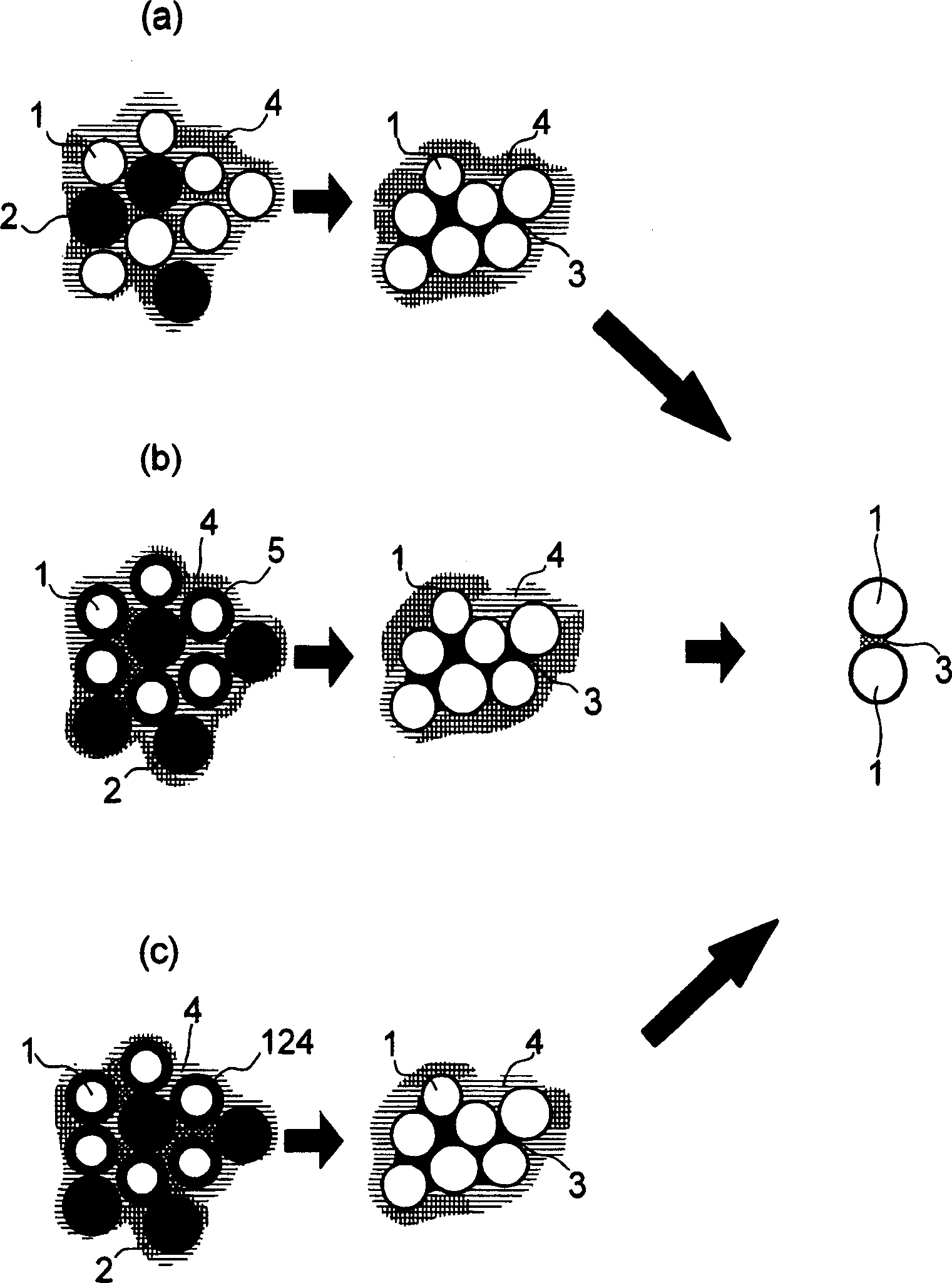
[0059] figure 1 (a) to figure 1 (c) shows a conceptual model of a bonding structure according to the present invention. The figure also shows a situation before welding and another situation after welding. figure 1 (a) shows a process in which Cu balls 1 (or balls of Ag, Au, CuSn alloy, etc.) with a particle size of about 30 micrometers are properly diffused through solder 4 and Sn-based particles with a particle size of about 30 micrometers. Example of solder paste for solder ball 2 (melting point: 232 degrees Celsius). When this solder paste is subjected to reflow at a temperature not lower than 250 degrees Celsius, the Sn-based solder ball 2 will melt, and the molten Sn3 will spread so that the molten Sn3 will wet the Cu ball 1 and appear relatively uniformly on the solder paste. Between Cu balls 1. Thereafter, the Cu balls 1 and the molten Sn3 react with each other so that the respective Cu balls 1 are connected to each other by means of a compound of Cu and Sn (mai...

Embodiment 2

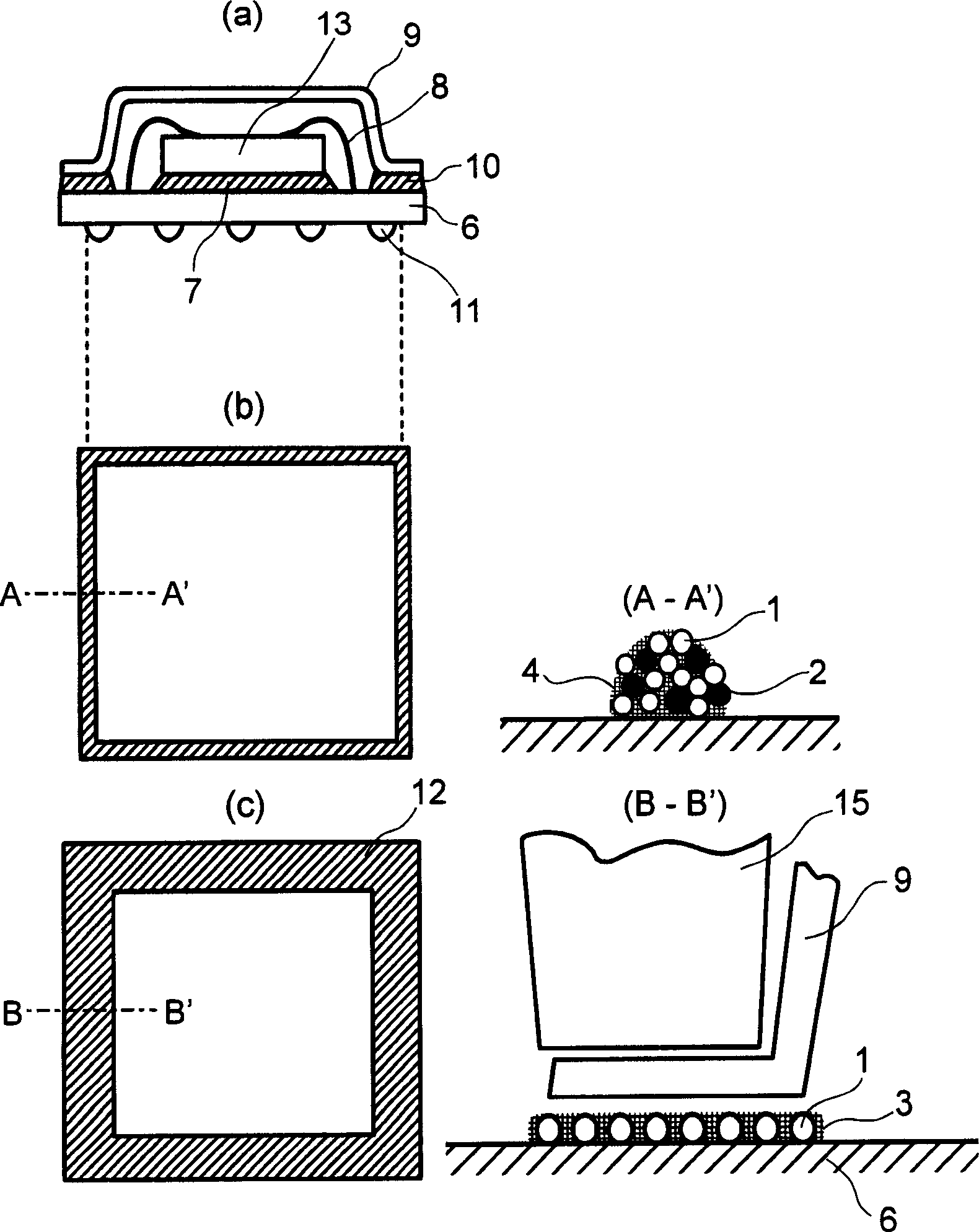
[0081] exist figure 2 In (a), the semiconductor device 13 is bonded to the bonding substrate 6 using an Au-20Sn solder 7 or the like. After wire bonding using gold wire 8 or the like, the outer peripheral portion of the cap 9 produced by applying NiAu plating to an Al plate, an iron Ni plate, or the like is reflowed using the above-mentioned non-clean type solder paste 10. bonded to the bonding substrate 6. In this case, when insulating characteristics are deemed important, bonding in a nitrogen atmosphere using solder with a chlorine-free flux is required. However, when wettability cannot be guaranteed, RMA type weakly reactive rosin can be used for encapsulation. It is not necessary to ensure complete encapsulation or sealing of the semiconductor device 13 . That is, if the solder has sufficient insulating characteristics, the semiconductor device 13 will not be adversely affected even when the semiconductor device 13 is held in the solder for a long time. The purpose o...

Embodiment 3

[0088] The solder paste according to the invention can also be used for figure 2 Die-in combination 7 shown in (a). After bonding the semiconductor device 13 using the solder paste according to the present invention, cleaning treatment and wire bonding are performed. In the prior art, die bonding is performed using Au-20Sn bonding. However, in view of the reliability of Au-20Sn solder, the use of Au-20Sn solder is limited to die mounting of small chips. In addition, when die-bonding is performed using a solder paste composed of lead-based solder, Pb-10Sn solder or the like is used. The bonding method according to the invention is also suitable for chips with larger areas. The greater the thickness of the bonding portion, the longer the service life and the higher the reliability. According to the present invention, the thickness can be increased by using high melting point balls each having a larger size. In the case of reduced thickness, this is done by reducing the siz...


PUM

PropertyMeasurementUnit
diameteraaaaaaaaaa
thicknessaaaaaaaaaa
thicknessaaaaaaaaaa

Abstract

In an electronic device realizing high-temperature terminal solder bonding in temperature-level bonding, the bonding portion between the semiconductor device and the substrate is formed by metal balls composed of Cu or the like and a compound composed of the metal balls and Sn, and Metal balls are held together by compounds.

Description

technical field [0001] The present invention relates to an electronic device using lead-free solder (solder that does not contain lead), and more particularly to an electronic device fabricated by a solder bonding method using a temperature hierarchy that can be efficiently mounted by an electronic device, etc. and other modules. Background technique [0002] When bonding with Sn lead-based solder, a temperature-level bonding method is used. In this combination technology, each component first uses the solder used for high-temperature soldering, such as lead-rich Pb-5Sn mass percent solder (melting point: 314-310 degrees Celsius) or Pb-10Sn mass percent solder (melting point: 302-275 degrees Celsius), soldering at a temperature between 330 degrees Celsius and 350 degrees Celsius, and then, using a solder used for low-temperature soldering, such as Sn-37Pb eutectic (183 degrees Celsius), to perform another soldering without melting the soldered part ( Hereinafter, "mass per...

Claims


Application Information

Patent Timeline
Patent Type & Authority Applications(China)
IPC IPC(8): B23K1/00B23K3/06B23K35/02B23K35/26B23K101/42C22C5/02C22C13/00H01L23/14H05K1/14H05K3/34
CPCB23K35/0244B23K35/262H01L2224/1134H01L2224/13144H01L2224/13147H01L2224/48247H01L2224/49171H01L2924/01012H01L2924/01046H01L2924/01078H01L2924/01079H01L2924/09701H01L2924/13091H01L2924/14H01L2924/15153H01L2924/1517H01L2924/15311H01L2924/16152H01L2924/19041H05K1/141H05K3/3463H05K2201/0215H05K2201/0218H05K2201/045H05K2201/10636H01L2924/00013H01L2924/01087H01L2924/01322H01L2224/32225H01L2224/32245H01L2224/48227H01L2224/48472H01L2224/73204H01L2224/73265H01L2924/19105H01L2224/45124H01L2224/45144H01L2924/01327H01L2224/48091H01L2924/10253H01L2224/16235H01L2924/181H01L24/73H01L2224/05573H01L2224/05568H01L2224/05166H01L2224/05169H01L2224/05144H01L2224/0508H01L2224/05611H01L2224/03828H01L2224/11334H01L24/11H01L24/13H01L2224/11472H01L2224/13023H01L2224/13018H01L2224/13582H01L2224/13644H01L2224/13655H01L2224/16227H01L2224/13118H01L2224/13155H01L2224/16058H01L24/03H01L24/05H01L2224/05548H01L2224/13024H05K3/3485Y02P70/50H01L2224/13099H01L2924/00H01L2924/00012H01L2924/00014H01L2224/05639H01L2224/05644H01L2224/05655H01L2224/05669H01L2924/014H01L2924/013H01L2924/0105H01L2924/01013H01L2224/16225H01L21/60H01L2224/16
Inventor 曾我太佐男秦英惠中塚哲也根岸干夫中嶋浩一远藤恒雄
Owner RENESAS ELECTRONICS CORP
Why Eureka
Try Eureka