Method for eliminating stress and damage while forming isolation component

A technology for eliminating stress and components, applied in electrical components, semiconductor/solid-state device manufacturing, circuits, etc., can solve problems such as stress damage in the active area of ​​semiconductor components and reduction in reliability of semiconductor components

Inactive Publication Date: 2003-10-22
MACRONIX INT CO LTD
View PDF0 Cites 9 Cited by
  • Summary
  • Abstract
  • Description
  • Claims
  • Application Information

AI Technical Summary

Problems solved by technology

For example, during trench etching, it may cause stress and damage to the active area...

Method used


Image

  • Method for eliminating stress and damage while forming isolation component
  • Method for eliminating stress and damage while forming isolation component
  • Method for eliminating stress and damage while forming isolation component

Examples


Embodiment Construction

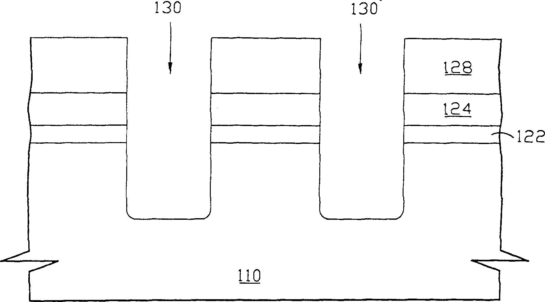
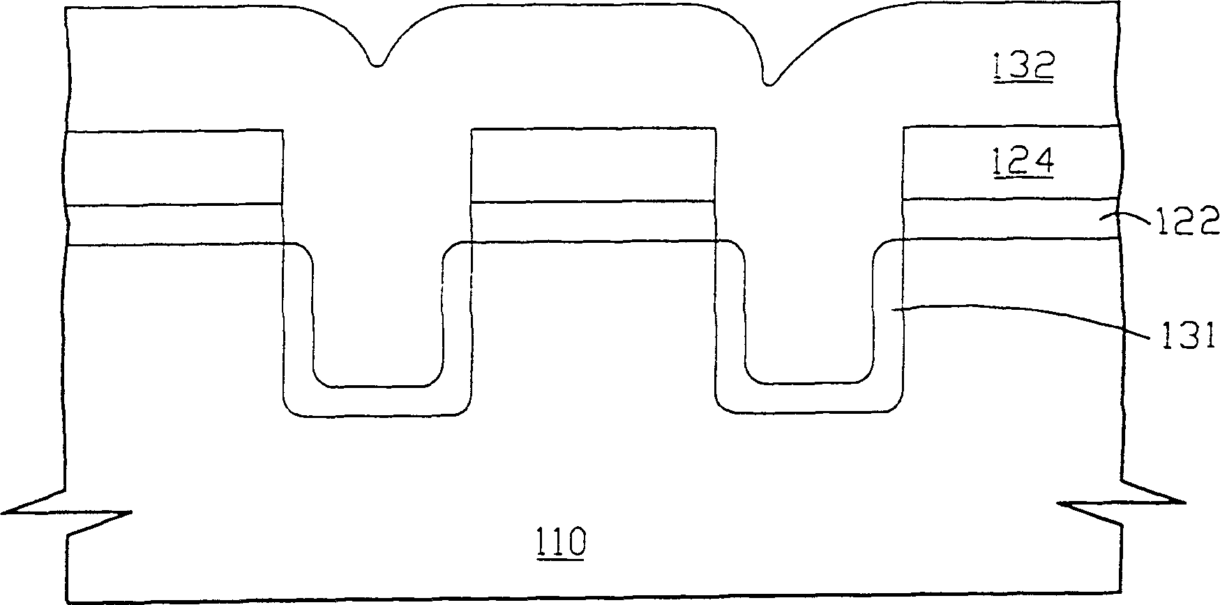
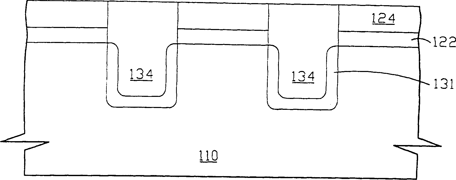
[0015] The method of the present invention can be widely applied to many semiconductor designs, and can be made using many different semiconductor materials. When the present invention describes the method of the present invention with a preferred embodiment, those who are familiar with this field should recognize Many steps can be changed, and materials and impurities can also be replaced, and these general replacements undoubtedly do not depart from the spirit and scope of the present invention.

[0016] Secondly, the present invention is described in detail as follows with schematic diagrams. When describing the embodiments of the present invention in detail, the cross-sectional view showing the semiconductor structure will not be partially enlarged according to the general scale in the semiconductor manufacturing process for the convenience of explanation, but it should not be used as a limitation. In addition, in actual production, the three-dimensional space dimensions of...


PUM


Abstract

This invention provides a method for eliminating stress and damage when forming a channeled isolation element including: providing a semi-conductor basic material to be etched to form a channeled structure, processing the channeled structure with high temperature annealing or quick heat annealing to eliminate stress of the channeled structure to reach the aim of avoiding the reduction of the reliability, semiconductive elements or annealing processing to a sidewall oxidation layer to eliminate the stress generated by the oxidation layer of the channeled structure.

Description

(1) Technical field [0001] The present invention relates to a method for eliminating stress and damage when forming isolation elements, in particular to a method for eliminating stress and damage when forming shallow trench isolation elements. (2) Background technology [0002] It is a common practice to use shallow-trench isolation technology to isolate components in integrated circuit manufacturing. Generally speaking, anisotropic etching process is used to form steep trenches on a semiconductor substrate using silicon nitride as a mask. Next, the trench is filled with oxide to form a shallow trench isolation device whose surface is at the same level as the surface of the substrate. [0003] Figure 1A to Figure 1D Schematic cross-sectional view of shallow trench isolation formed by conventional methods. refer to Figure 1A As shown, a pad oxide layer 122 (pad oxide layer) is formed on the silicon substrate 110 to protect the silicon substrate 110, and the pad oxide lay...

Claims


Application Information

Patent Timeline
IPC IPC(8): H01L21/324H01L21/76
Inventor 许淑雅
Owner MACRONIX INT CO LTD
Why Eureka
Try Eureka