Semiconductor device and capacitance measuring method

A capacitance measurement and semiconductor technology, which is applied in semiconductor/solid-state device testing/measurement, semiconductor devices, semiconductor/solid-state device manufacturing, etc., can solve problems such as difficult, difficult separation of wiring capacitance components, inconsistent gate lengths, etc.

Inactive Publication Date: 2003-12-17
PANASONIC CORP +1
View PDF0 Cites 14 Cited by
  • Summary
  • Abstract
  • Description
  • Claims
  • Application Information

AI Technical Summary

Problems solved by technology

[0053] (2) Questions about the monitoring of wiring capacitance
[0060] like Figure 27 As shown, as components of the wiring capacitance, in addition to the inter-wiring capacitance C1 in the same wiring layer, there is also the capacitance Cv between other wiring layers. However, in the conventional wiring pattern, it is not easy to separate the components of these wiring capacitances.
[0061] (3) Questions about the measurement of input and output capacitances of standard cells
[0065] (4) Questions about monitoring of gate length inconsistency
[0067] In the CBCM method, if the measurement frequency f is increased, the proportion of the gate leakage in the measurement current will be relatively reduced. Figure 22 For the gate control signal shown, there is an upper limit in the measurement frequency f
In addition, the measurement device itself can operate at a frequency of several 10MHz to 100MHz, but the resonance frequency in the measurement system (especially the coaxial signal line) is around several MHz, so if the tolerance is considered, the measurement frequency, 1MHz becomes the limit , it is difficult to remove the effect of gate leakage from the measured value of capacitance

Method used


Image

  • Semiconductor device and capacitance measuring method
  • Semiconductor device and capacitance measuring method
  • Semiconductor device and capacitance measuring method

Examples


Embodiment 1

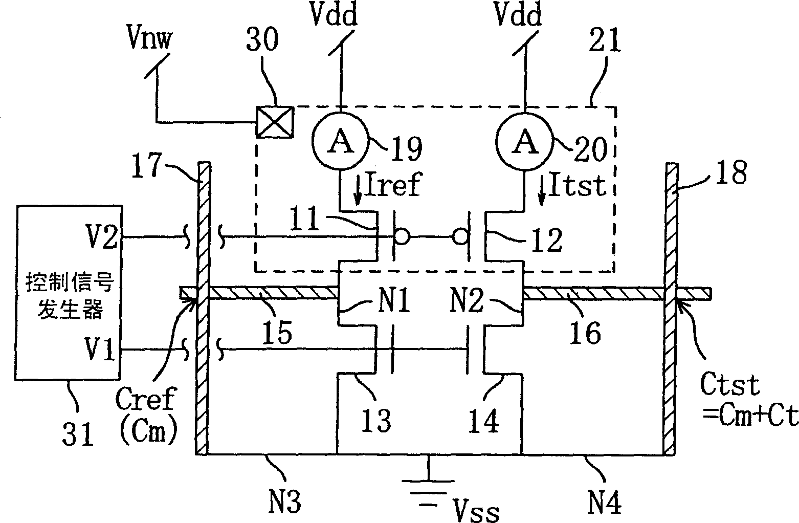
[0133] figure 1 It is a circuit block diagram schematically showing the circuit configuration of the CBCM measurement device (semiconductor device of the present invention) used in Embodiment 1 of the present invention.

[0134] Such as figure 1 As shown, the CBCM measuring device of this embodiment has: a reference PMIS transistor 11 , a test PMIS transistor 12 , a reference NMIS transistor 13 , and a test NMIS transistor 14 . And, the reference PMIS transistor 11 and the test PMIS transistor 12 have a gate length and a gate width equal to each other in the mask size, and the reference NMIS transistor 13 and the test NMIS transistor 14 have a gate length and a gate width equal to each other. mask size. Furthermore, in a semiconductor substrate (wafer), more semiconductor devices according to the present invention are arranged on scribe lines than in chip regions.

[0135] The reference PMIS transistor 11 and the reference NMIS transistor 13 are arranged in series between...

Embodiment 2

[0159] In this example, using the figure 1 The circuit configuration shown is the CBCM measurement setup.

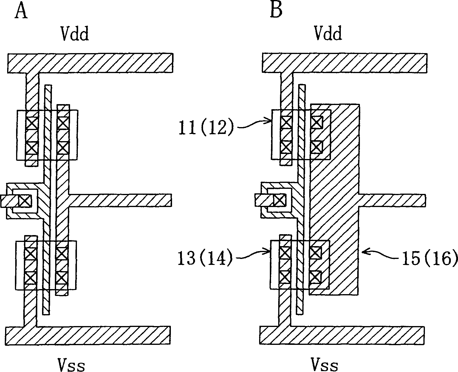
[0160] Figure 5 (a) and (b) are plan views showing the structures of the first and second conductor parts for reference and the structures of the first and second conductor parts for testing in Example 2, respectively. Here, using the same mask of the pattern, a Figure 5 The reference second conductor portion 17A and the test second conductor portion 18A shown in (a) and (b). The first reference conductor portion 15A and the first test conductor portion 16A were formed using a mask having different lengths L1, L2 of one line 15a, 16a in the center and the same size and pattern in other portions. Also, when the basic length corresponding to the target capacitance is Ltar, the shapes of the respective conductor portions 15A, 16A, 17A, 18A are set such that the following expressions (3) to (5) hold:

[0161] L1=4·Ltar...(3)

[0162] L2=5·Ltar...(4)

[0163] L2-L1=L...

Embodiment 3

[0182] Figure 7 It is a circuit block diagram schematically showing the circuit configuration of the CBCM measurement device used in Embodiment 3 of the present invention.

[0183] Such as Figure 7 As shown, the CBCM measuring device of this embodiment has four PMIS transistors 51a-51d and four NMIS transistors 52a-52d. Furthermore, the respective PMIS transistors 51 a to 51 d have a mask size whose gate length and gate width are equal to each other, and the NMIS transistors 52 a to 52 d have a mask size whose gate length and gate width are equal to each other.

[0184] The PMIS transistors 51a to 51d and the NMIS transistors 52a to 52d are arranged in series between the terminal (terminal pad) to which the power supply voltage Vdd is supplied and the terminal (terminal pad) to which the ground voltage Vss is supplied. That is, the power supply voltage Vdd is supplied to the sources of the PMIS transistors 51a to 51d, and the ground voltage Vss is supplied to the sources o...


PUM


Abstract

The invention provides a semiconductor device with the measurement accuracy of capacity or a method for measuring the capacity. A CBCM measurement device comprises PMIS transistors 11, 12, NMIS transistors 13, 14, a first conductor 15 for reference connected to a first node N1, a second conductor 17 for reference forming a dummy capacitor between the first conductor 15 for reference and itself, a first conductor for a test connected to a second node, and a second conductor 18 for the test forming a test capacitor between the first conductor for the test and itself. The capacity of a target capacitor in the test capacitor is measured from a current flowing in the first and the second nodes by controlling the ON-OFF action of each transistor with control voltages V1, V2. The measurement accuracy of the capacity is improved by increasing dummy capacity.

Description

technical field [0001] The present invention relates to a semiconductor device having a function of generally measuring wiring capacitance, gate capacitance, and junction capacitance. Background technique [0002] In recent years, along with densification of semiconductor devices, the ratio of circuit delay to wiring length based on wiring capacitance has increased, and at the same time, variations in parameters defining wiring have increased due to inconsistencies in process manufacturing conditions and the like. As a result, the problem of increased inconsistency in circuit delay between semiconductor devices becomes prominent, and monitoring of inconsistency in wiring capacitance becomes important. [0003] However, in conventional measurement of wiring capacitance using an LCR meter, a large-area TEG pattern is required to maintain measurement accuracy, so it is difficult to monitor the inconsistency of wiring capacitance in a product chip. [0004] Therefore, the CBCM ...

Claims


Application Information

Patent Timeline
Patent Type & Authority Applications(China)
IPC IPC(8): G01R27/26G01R31/27G01R31/28G01R31/312H01L21/66H01L21/822H01L27/04
CPCG01R31/312G01R31/275
Inventor 山下恭司海本博之小林睦大谷一弘国清辰也永久克己
Owner PANASONIC CORP
Why Eureka
Try Eureka