Electrostatic discharge protecter and its producing method

A technology of electrostatic discharge protection and manufacturing method, which is applied in semiconductor/solid-state device manufacturing, circuits, electrical components, etc., and can solve problems such as adverse electrostatic discharge performance and increasing parasitic capacitance and capacitance value.

Inactive Publication Date: 2004-03-10
SEMICON MFG INT (SHANGHAI) CORP +1
View PDF0 Cites 9 Cited by
  • Summary
  • Abstract
  • Description
  • Claims
  • Application Information

AI Technical Summary

Problems solved by technology

The P-type doped region 119 is formed "in one block" under the drain region 115. Although it can help the bipolar transistor to conduct, it will increase the capacitance of the parasitic capacitance, which is not conducive to the performance of electrostatic discharge.

Method used


Image

  • Electrostatic discharge protecter and its producing method
  • Electrostatic discharge protecter and its producing method
  • Electrostatic discharge protecter and its producing method

Examples


Embodiment Construction

[0021] 3A3E show a flow chart of manufacturing an ESD protection device according to an embodiment of the present invention.

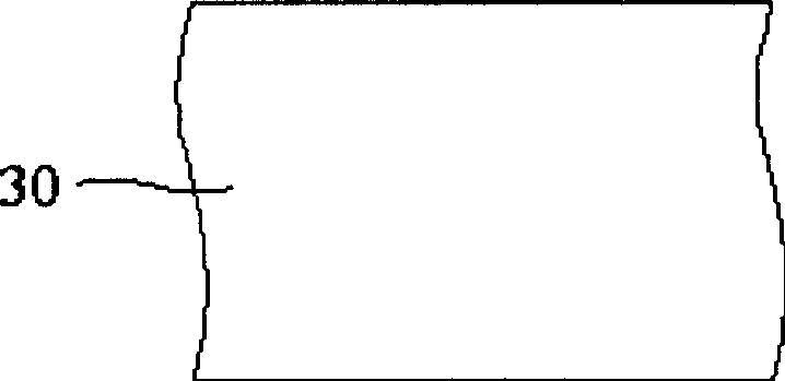
[0022] First, if Figure 3A As shown, a silicon-substrate 30 is provided.

[0023] Next, if Figure 3B As shown, the dopant dose is about 1e12cm -3 -6e13cm -2 A boron ion implantation process is performed to form a P-type well region 312 .

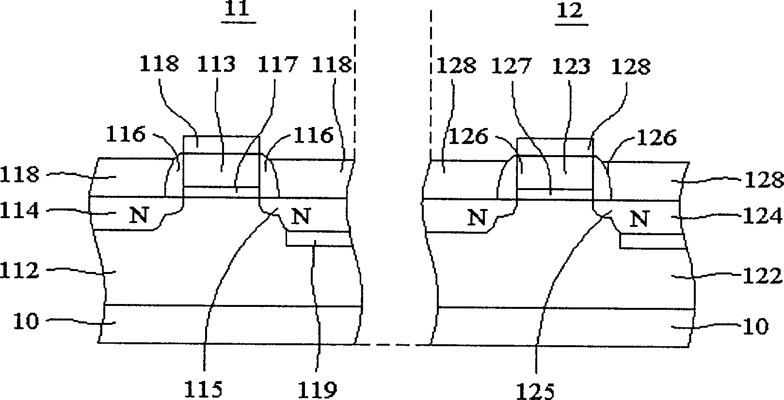
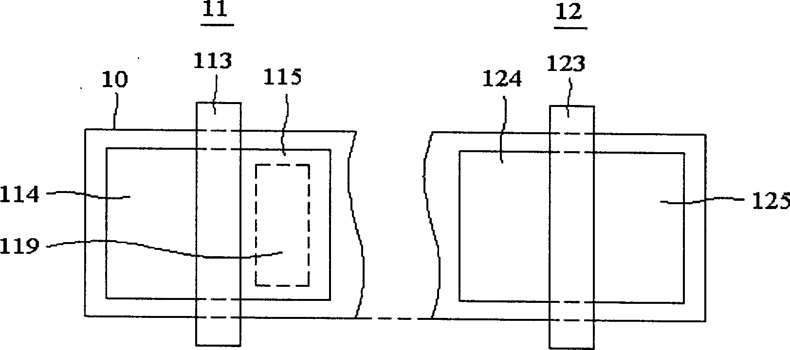
[0024] Then, if Figure 3C As shown, the doping dose in the dP well region 312 is about 1e12cm 3 -6e13cm -2 A boron ion implantation process is performed to form a plurality of doped regions 319 . The shape and arrangement of the doped region 319 are as follows: Figure 4A~4D As shown, it may be arranged in a row in a strip shape and parallel to the gate 313 to be formed later, two rows in a strip and in a direction parallel to the gate 313 to be formed later, and one row in a strip shape and are arranged in a direction perpendicular to and surrounding the gate 313 which will be formed later.

[0025] Nex...


PUM


Abstract

The method includes following steps: providing a substrate, forming a trap area; a doping area is formed in the trap area, and a grid electrode is formed above the grid electrode; a source electrode area and a drain electrode area adjacent to the doping area are formed in the trap on two sides of the grid electrode.

Description

technical field [0001] The present invention relates to an electrostatic discharge protection device and its manufacturing method, in particular to an electrostatic discharge protection device that provides a plurality of doped regions for reducing breakdown voltage in the well area of ​​the high-voltage electrostatic discharge protection circuit area and methods of manufacture thereof. Background technique [0002] For integrated circuits, electrostatic discharge (Electrostatic Discharge, ESD) will cause damage to the integrated circuits, making the integrated circuits unable to operate normally. At present, in the manufacture of integrated circuits, many methods and devices for solving the electrostatic discharge problem have been proposed. [0003] In integrated circuits, in order to prevent electrostatic discharge from causing damage to the internal main circuit, an electrostatic discharge protection device is generally made between the internal circuit and the input / ou...

Claims


Application Information

Patent Timeline
Patent Type & Authority Applications(China)
IPC IPC(8): H01L21/77H01L23/60
Inventor 俞大立
Owner SEMICON MFG INT (SHANGHAI) CORP
Why Eureka
Try Eureka