

Pattern formation material, water-soluble material and pattern formation method
A technology of water-soluble materials and water-soluble films, which can be used in photosensitive materials used in optomechanical equipment, photoplate-making process of patterned surface, optics, etc., can solve the problems of resist pattern deterioration and productivity reduction, and avoid Effects of reduction in strength, reduction in productivity, and prevention of deterioration
- Summary
- Abstract
- Description
- Claims
- Application Information
AI Technical Summary
Problems solved by technology
Method used
Image

Examples
Embodiment approach 1
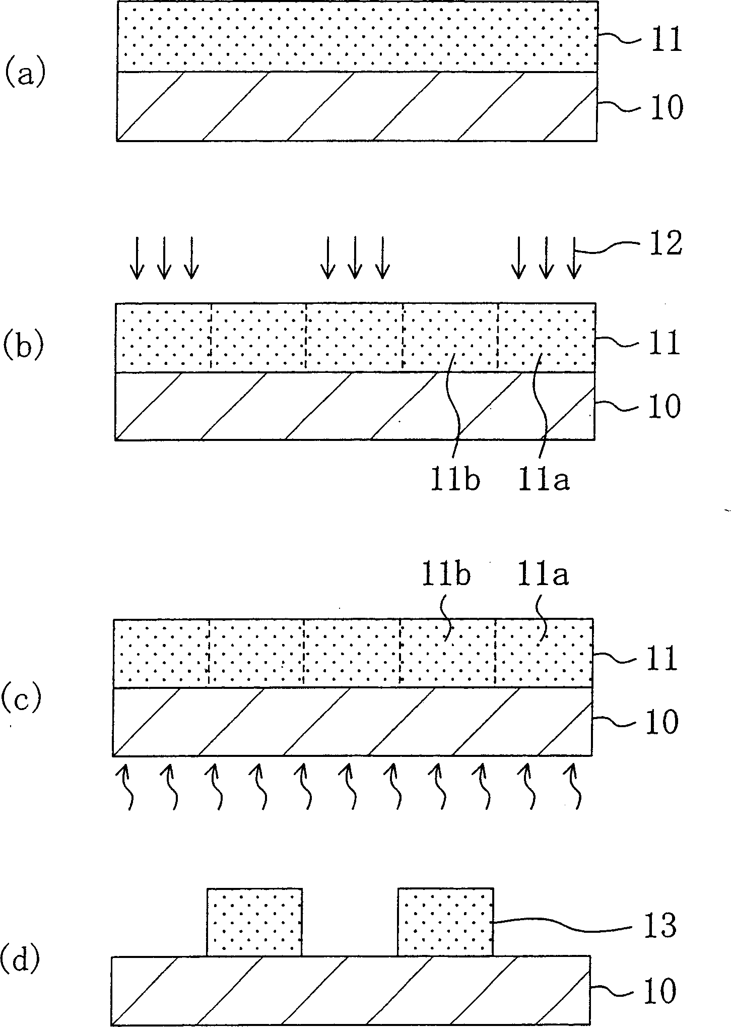
[0057] Below, refer to figure 1 (a) to (d) The pattern forming method according to Embodiment 1 of the present invention will be described.
[0058] First, a chemically amplified resist material having the following composition was prepared.
[0059] Poly[(tert-butyl methacrylate)-(mevalonolactone methacrylate)] (tert-butyl methacrylate: mevalonolactone methacrylate=50mol%: 50mol%) (polymer )
[0060] 2g
[0061] Triphenylsulfonium trifluoride (triphenylsulphoniumtriflate) (acid generator) 0.08g
[0062] Granular egret G2c [manufactured by Takeda Pharmaceutical Co., Ltd.] (crushed charcoal) 0.16g
[0063] Propylene glycol monomethyl ether acetate (solvent) 20g
[0064] Then if figure 1 As shown in (a), the chemically amplified resist material is spin-coated on the semiconductor substrate 10 to form a resist film 11 with a thickness of 0.2 μm.
[0065] Then, if figure 1 As shown in (b), the resist film 11 is irra...
Embodiment approach 2
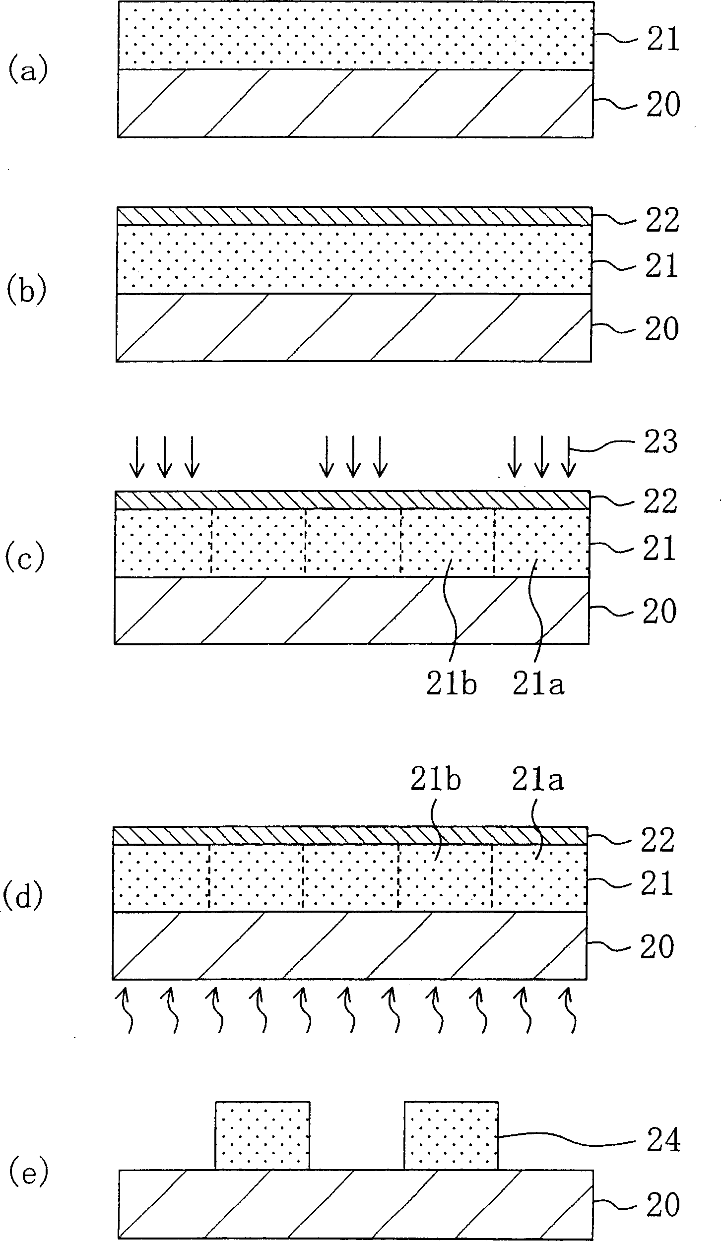
[0072] Below, refer to figure 2 (a) to (e) The pattern forming method according to Embodiment 2 of the present invention will be described.
[0073] First, a chemically amplified resist material having the following composition was prepared.
[0074] Poly[(tert-butyl methacrylate)-(mevalonolactone methacrylate)] (tert-butyl methacrylate: mevalonolactone methacrylate=50mol%: 50mol%) (polymer )
[0075] 2g
[0076] Triphenylsulfonium trifluoride (triphenylsulphoniumtriflate) (acid generator) 0.08g
[0077] Propylene glycol monomethyl ether acetate (solvent) 20g
[0078] Then if figure 2 As shown in (a), the chemically amplified resist material is spin-coated on the semiconductor substrate 20 to form a resist film 21 with a thickness of 0.2 μm.
[0079] Then, if figure 2 As shown in (b), a water-soluble material having the following composition was spin-coated on the resist film 21 to form a water-soluble film 22 ha...
Embodiment approach 3
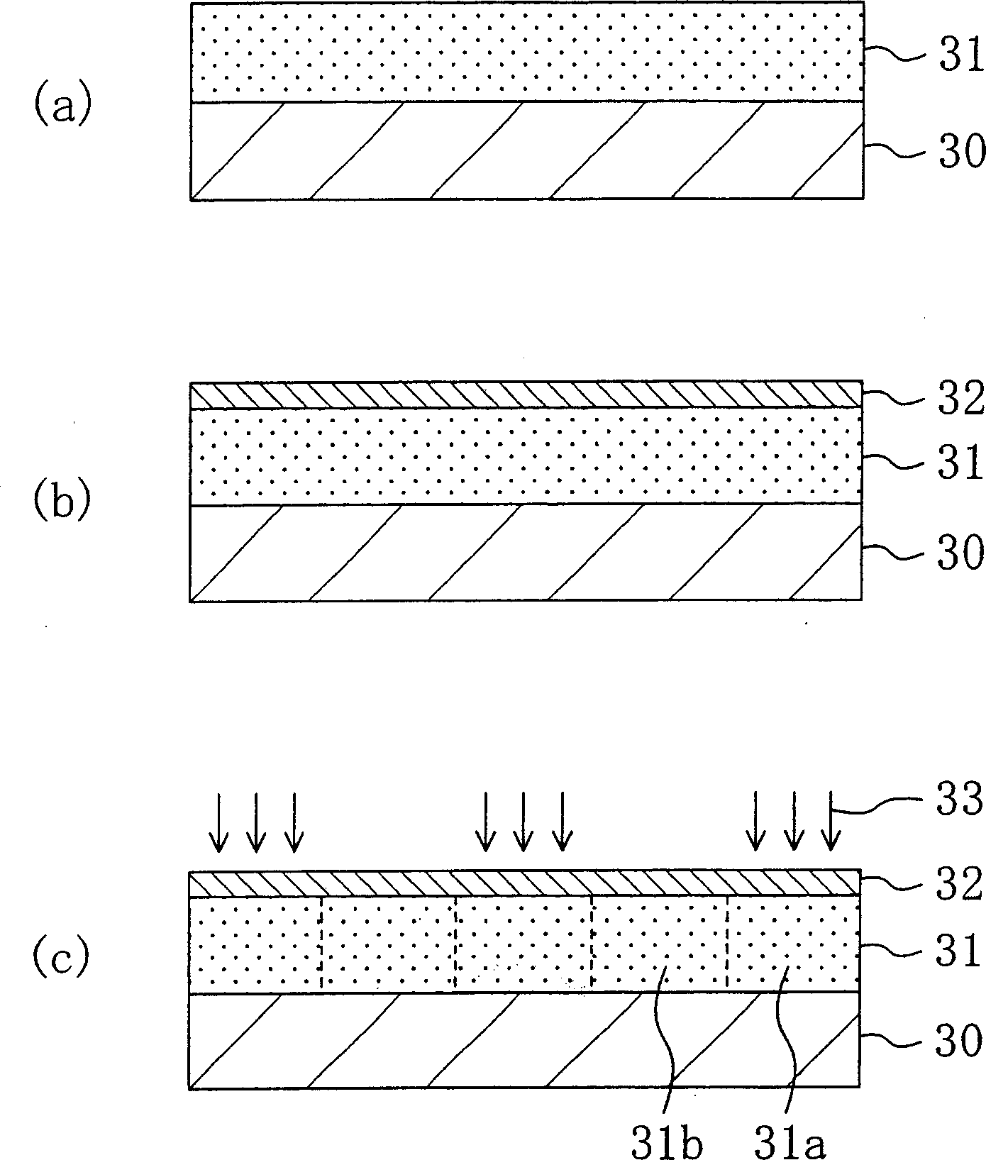
[0089] Below, refer to image 3 (a)~(c) and Figure 4 (a) to (c) The pattern forming method according to Embodiment 3 of the present invention will be described.
[0090] First, a chemically amplified resist material having the following composition was prepared.
[0091] Poly[(tert-butyl methacrylate)-(mevalonolactone methacrylate)] (tert-butyl methacrylate: mevalonolactone methacrylate=50mol%: 50mol%) (polymer )
[0092] 2g
[0093]Triphenylsulfonium trifluoride (triphenylsulphoniumtriflate) (acid generator) 0.08g
[0094] Propylene glycol monomethyl ether acetate (solvent) 20g
[0095] Then as image 3 As shown in (a), the chemically amplified resist material is spin-coated on the semiconductor substrate 30 to form a resist film 31 with a thickness of 0.2 μm.
[0096] Then, if image 3 As shown in (b), a water-soluble material having the following composition was spin-coated on the resist film 31 to form a water...
PUM
| Property | Measurement | Unit |
|---|---|---|
| thickness | aaaaa | aaaaa |
Abstract
Description
Claims
Application Information