Magnetic body, apparatus using the same and its mfg. method

A magnet and non-magnetic technology, applied in the direction of inductance/transformer/magnet manufacturing, magnetic objects, magnetic materials, etc., can solve the problems of poor bonding ability of adjacent substances, miniaturization, high integration, and reduction of circuit production steps. Problems such as making magnetic substances

Inactive Publication Date: 2004-05-05
NIPPON TELEGRAPH & TELEPHONE CORP
View PDF1 Cites 14 Cited by
  • Summary
  • Abstract
  • Description
  • Claims
  • Application Information

AI Technical Summary

Problems solved by technology

[0003] Because all these magnetic substances include magnetic metals, the product processing of these magnetic substances such as when using semiconductors such as silicon, chromium, selenium (GaAs) on the LSI (Large Scale Integration) sublayer to manufacture magnetic devices, encounters various problems. Various problems, such as the poor binding ability of adjacent substances themselves
[0004] Therefore, each circuit has to be made into discrete parts different from electronic components, for example, transistors are formed on LSI sublayers, which brings a series of obstacles to miniaturization, high integration, and reduction of production steps of circuits
[0005] Also, since semiconductor clusters, carbon clusters, and metal clusters chemically synthesized from non-magnetic substances are not magnetic, only a combination of these components cannot be made into a magnetic substance

Method used


Image

  • Magnetic body, apparatus using the same and its mfg. method
  • Magnetic body, apparatus using the same and its mfg. method
  • Magnetic body, apparatus using the same and its mfg. method

Examples


no. 1 example

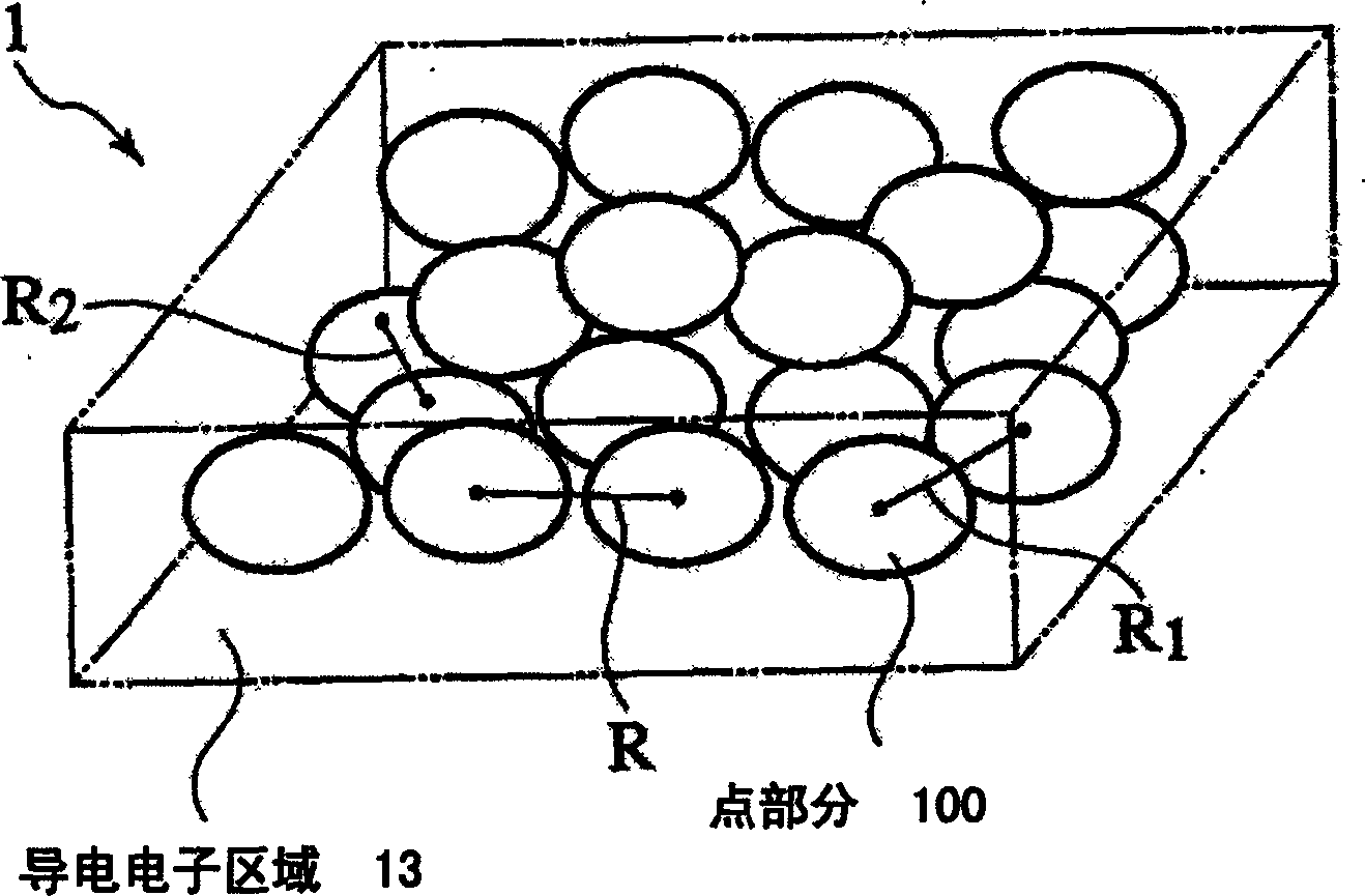
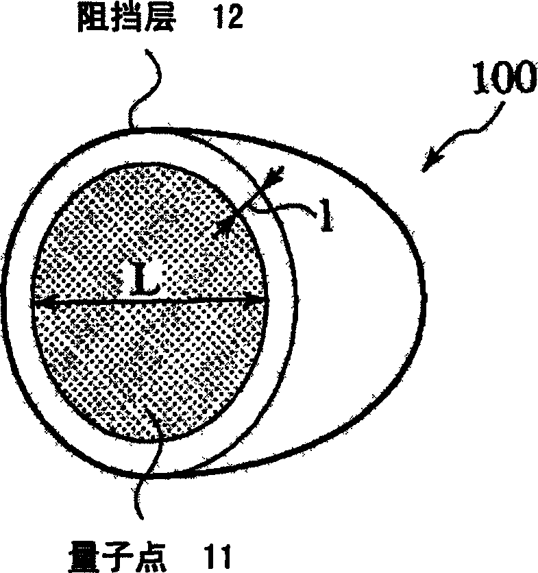
[0114] figure 1 Shown is an explanatory diagram of the magnet structure of the first embodiment of the present invention. in addition, figure 2 shown as figure 1 Illustrative diagrams of the structure of one point part 100, as shown in these figures, the magnet 1 has the structure of multi-quantum dots 11, and the multi-quantum dots 11 form local electron regions with local spins, wherein at least one electron is confined, and the multi-quantum dots 11 overlap each other at the dot portion 100, surrounded by a barrier layer 12 (barrier potential region), electrons pass through the barrier layer and are confined within each quantum dot 11, in a conduction electron region 13, consisting of a conduction electron system, which The energy is less than that of the barrier layer 12 .

[0115] At the same time, there is no contrary opinion that the energy magnitude of the quantum dot 11 in the electron localized region and the conduction electron region 13 is an arbitrary value. ...

no. 2 example

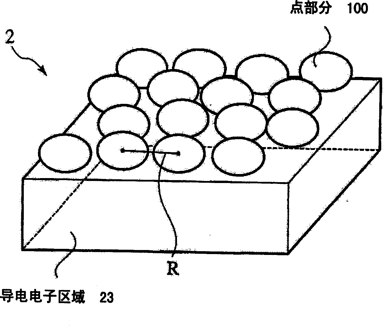
[0142] Figure 6 Shown is an explanatory diagram of a magnet structure of a second embodiment of the present invention. Figure 6 The illustrated magnet 5 attempts to use a two-dimensional conducting electron gas that forms in the two-dimensional electron system interface 56, such as compound semiconductors composed of GaAs, aluminum-cadmium-selenium (AlGaAs), and silicon and silicon oxides. Different interfaces for the commutation layer of silicon MOS (Metal Oxide Semiconductor) transistors.

[0143] However, Figure 6 Shown at the boundary between the semiconductor 54 and the semiconductor 55, a two-dimensional electronic system interface 56 is formed, in one case, the two-dimensional electronic system interface 56 includes different interfaces of the above-mentioned semiconductor compound, the semiconductor 54 is composed of GaAs, the semiconductor 55 (insulating layer) is composed of AlGaAs. In this case, GaAs and AlGaAs can also be reversed. It is also possible, in a ...

no. 3 example

[0151] Figure 8 Shown is an explanatory diagram of a magnet structure of a third embodiment of the present invention. The magnet 6 shown in the figure is manufactured by an etching method or a semiconductor selective growth method. In particular, by etching, a semiconductor is processed to remove a portion of it to eventually form Figure 8 The structure shown, by means of which the electrodes transport allows the accumulation of the electrodes within this wire domain of quantum, the cross-section of this wire area represented in the same figure by the particular rhombus shape, thus forming the quantum dot portion 61 . At the same time, the size of the quantum dot portion 61 is also equal to the size of the quantum dot portion of the first embodiment and the second embodiment. In addition, in Figure 8 In , all the cross-sectional areas forming the quantum dot portion 61 are shown and described in the same rhombus shape. Of course, it can be understood that the quantum do...


PUM

PropertyMeasurementUnit
thicknessaaaaaaaaaa

Abstract

A magnetic body composed of non-magnetic material, includes a plurality of localized electron regions in each of which at least one electron is confined to form a localized spin, a barrier potential region having a higher energy than a Fermi energy of an electron in the localized electron region and permitting an electron to be confined in the respective localized electron regions, and a conductive electron region including a conductive electron system having a lower energy than an energy of the barrier potential region, wherein the respective localized electron regions are disposed separate from one another via the barrier potential region and the conductive electron region.

Description

technical field [0001] The present invention relates to a magnet, a magnetic device using the magnet, and a manufacturing method of the magnet. Background technique [0002] Generally, magnetic storage media and magnetic sensors are manufactured from magnets composed of magnetic substances, such as natural magnets (eg, magnets: Fe 3 o 4 ), alloy magnets (such as chromium steel and high cobalt steel), magnets are composed of alnico alloys, ferrites and rare earths. [0003] Because all these magnetic substances include magnetic metals, the product processing of these magnetic substances such as when using semiconductors such as silicon, chromium, selenium (GaAs) on the LSI (Large Scale Integration) sublayer to manufacture magnetic devices, encounters various problems. Various problems, such as the poor binding ability of adjacent substances themselves. [0004] Therefore, each circuit has to be made in discrete parts different from electronic components, for example, trans...

Claims


Application Information

Patent Timeline
Patent Type & Authority Applications(China)
IPC IPC(8): H01F1/00H01F10/00
CPCH01F10/007H01F1/009B82Y25/00H01F1/404H01F10/193H01F41/302Y10S977/932
Inventor 田村浩之高柳英明
Owner NIPPON TELEGRAPH & TELEPHONE CORP
Why Eureka
Try Eureka