
High frequency module

A high-frequency module and high-frequency technology, applied in high-frequency matching devices, printed circuits, waveguides, etc., can solve problems such as deterioration of high-frequency characteristics, influence of high-frequency wave characteristics, and deterioration of characteristics, so as to maintain high-frequency connectivity and continuity performance, improving high-frequency characteristics, and reducing unevenness

Inactive Publication Date: 2004-06-23
SONY CORP
View PDF1 Cites 9 Cited by
  • Summary
  • Abstract
  • Description
  • Claims
  • Application Information

AI Technical Summary

Problems solved by technology

In this high-frequency module substrate 200, since the ground patterns 209a, 209b are connected to the ground pattern on the base substrate side through the metal-plated interlayer as described above, the resistance component and the inductance component such as the metal-plated interlayer affect the high-frequency wave. sexual problems
In addition, in the high-frequency module substrate 200, since capacitance components are generated between each passive element and the ground pattern on the base substrate side, problems such as a decrease in the Q value of the self-resonant frequency and a quality factor, and deterioration of characteristics occur.
[0019] Furthermore, due to Figure 5 The high-frequency module substrate 200 shown has a ground pattern defining a ground plane on the base substrate side as described above, and the transmission line 204 constitutes a microstrip transmission line. uneven thickness
Thus, if Figure 5 In the high-frequency module substrate 200 shown, it is difficult to form the high-frequency circuit part with high-precision molding on the base substrate part, and problems such as deterioration of high-frequency characteristics arise.

Method used


Image

  • High frequency module
  • High frequency module
  • High frequency module

Examples


Embodiment Construction

[0035] Hereinafter, embodiments of the present invention will be described in detail with reference to the drawings.

[0036] The high-frequency module related to the present invention has an information communication function and a storage function, and is applied to, for example, a personal computer, a mobile phone, a portable information terminal device or a portable audio device installed in a small-scale wireless communication system specification with a carrier frequency band specification of 5 GHz In various electronic equipment, or as an optional plug-in, pull-out ultra-small communication function components, etc.

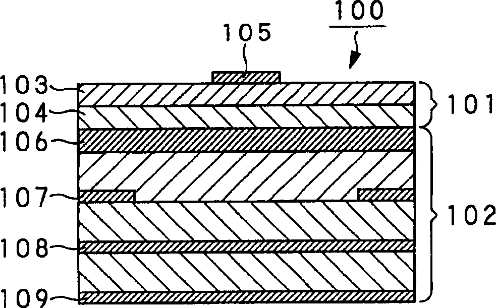
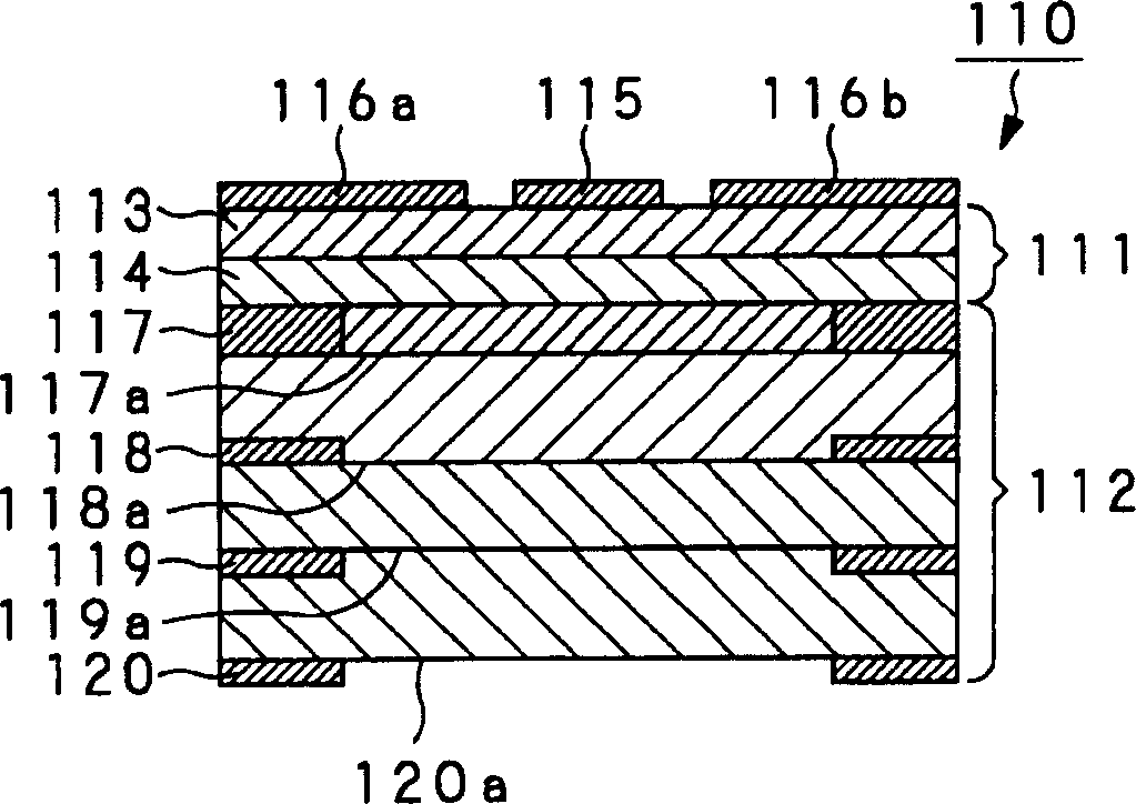
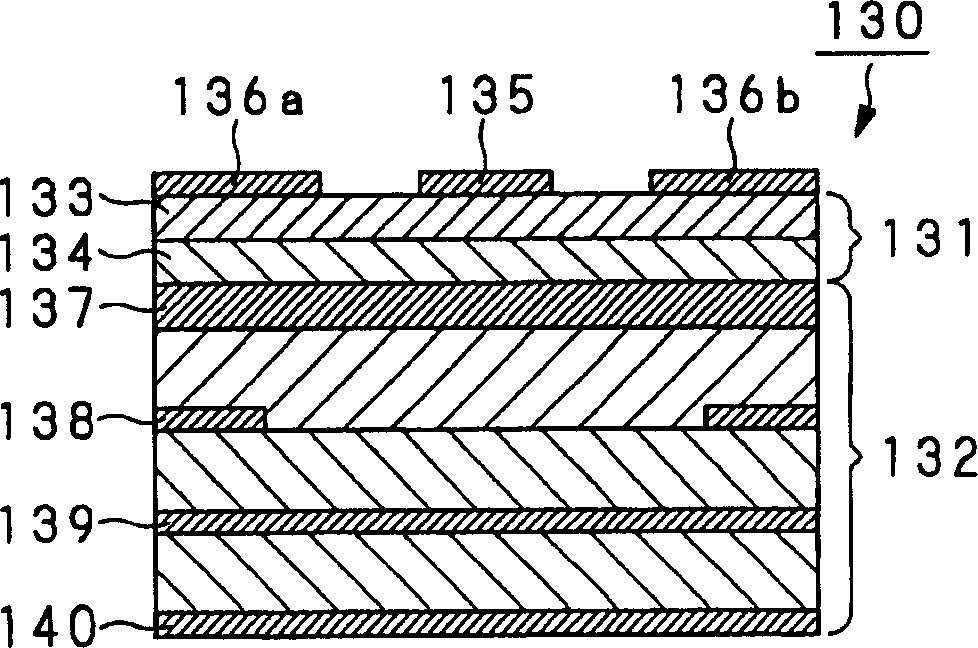
[0037] Related to the high frequency module 1 of the present invention, such as Figure 6 As shown, it is composed of a base substrate part 2 and a high-frequency circuit 3 laminated on the base substrate part 2 . On the surface of the high-frequency circuit unit 3, a semiconductor chip 4 having a peripheral circuit function such as a high-frequency trans...


PUM


Abstract

The present invention provides a high frequency module having a base substrate unit ( 2 ) which has its uppermost layer planarized to form a buildup-forming surface ( 16 ), a high frequency circuit unit ( 3 ) having multiple wiring layers which are formed on the base substrate unit ( 2 ), each of which layers has a wiring pattern and film elements formed on a dielectric insulating layer thereof, whose uppermost wiring layer ( 17 ) has plural lands ( 22 ) and ground patterns ( 20 ) formed thereon together with the wiring pattern and inductor elements ( 19 ), and a semiconductor chip ( 4 ) mounted on the wiring layer ( 17 ) of the high frequency circuit unit ( 3 ). Transmission lines ( 24 ) to connect the inductor elements ( 19 ) and lands ( 22 ) which are formed on the wiring layer ( 17 ) are directed within hollowed pattern regions ( 20 c) formed at the ground pattern ( 20 ) to constitute coplanar type transmission lines.

Description

technical field [0001] The present invention relates to a high-frequency module used in a wireless communication component with a wireless communication function and a storage function. [0002] This application claims priority based on Japanese Patent Application Serial No. 2002-062250 filed on March 7, 2002 in Japan, and this application refers to and cites this application. Background technique [0003] Various information communication systems With the development of various communication terminal equipment and data processing systems, through the installation of ISDN (Integrated Service Digital Network: Integrated Service Digital Network) and digital transmission and other service networks, the use of fixed equipment to mobile equipment Information reception, delivery of is attracting attention. A wireless communication component with a wireless communication function and a storage function is installed in the communication device. The wireless communication component...

Claims


Application Information

Patent Timeline
Patent Type & Authority Applications(China)
IPC IPC(8): H01L23/12H01L23/498H01L23/66H01P3/08H05K1/02H05K1/16H05K3/46
CPCH05K3/4602H05K3/4688H01L2924/19105H05K1/165H05K1/0237H05K1/024H01L2924/15311H05K2201/09336H05K1/0219H01L23/66H05K2201/0715H05K2201/10674H01L2224/16225H01L2223/6677H01L2924/19015H01L23/49838H01L25/16H05K3/46H05K1/02
Inventor 小濑村孝彦奥洞明彦
Owner SONY CORP
Learn More