Manufacturing method of semiconductor device and semiconductor device

A manufacturing method and semiconductor technology, which are applied in the fields of semiconductor/solid-state device manufacturing, semiconductor devices, and semiconductor/solid-state device components, etc., can solve the problems of many processes and high costs, and achieve simplified manufacturing processes, improved production capacity, and reduced costs. Effect

Inactive Publication Date: 2004-08-04
SEIKO EPSON CORP
View PDF3 Cites 8 Cited by
  • Summary
  • Abstract
  • Description
  • Claims
  • Application Information

AI Technical Summary

Problems solved by technology

[0006] However, in the above-mentioned prior art, when forming passive components, spraying method, photolithography method, electric field plating method, etc. are used as specific manufacturing methods, and there are problems in that many steps are required and the cost is high.

Method used


Image

  • Manufacturing method of semiconductor device and semiconductor device
  • Manufacturing method of semiconductor device and semiconductor device
  • Manufacturing method of semiconductor device and semiconductor device

Examples


Embodiment 1

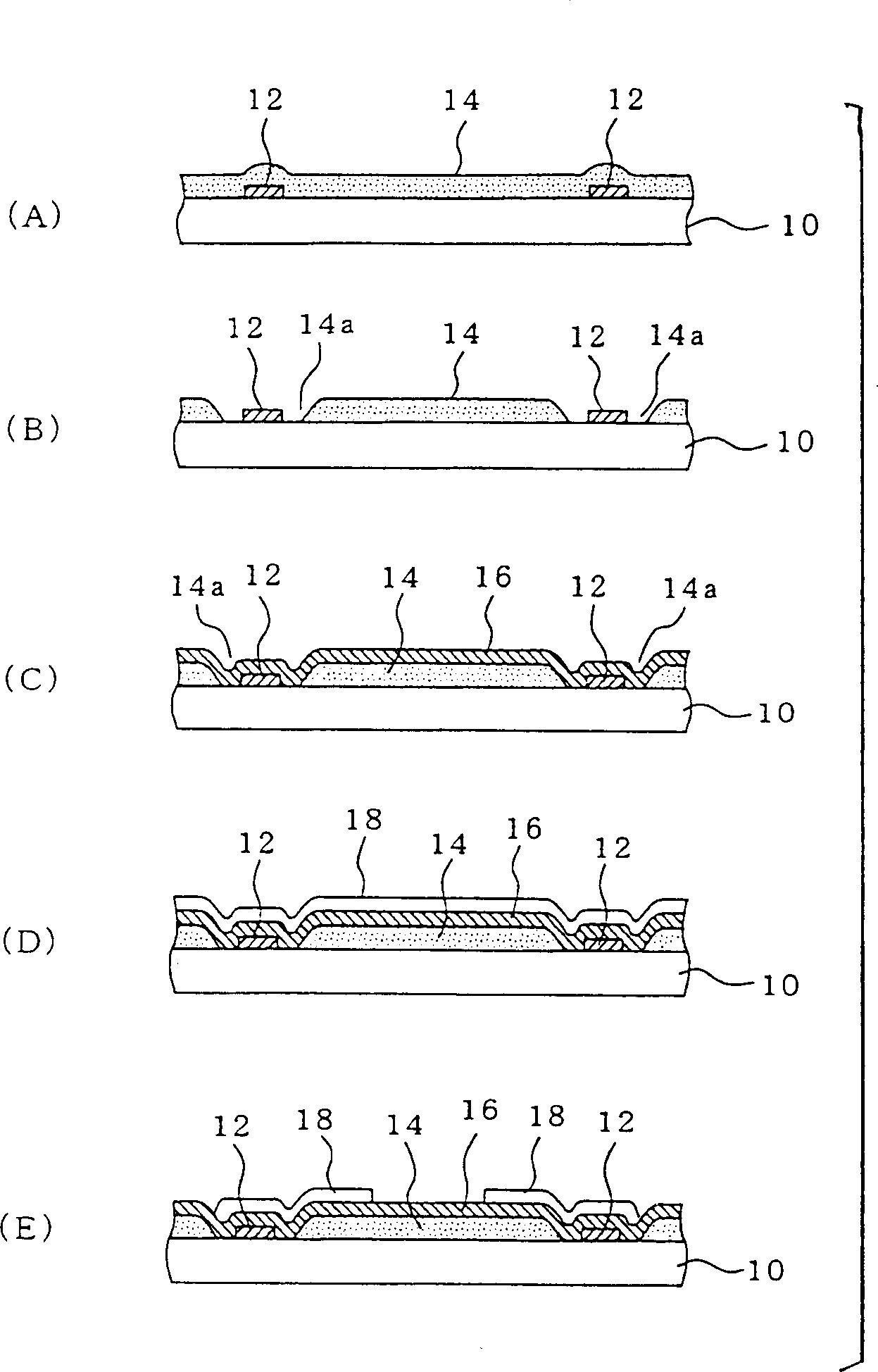
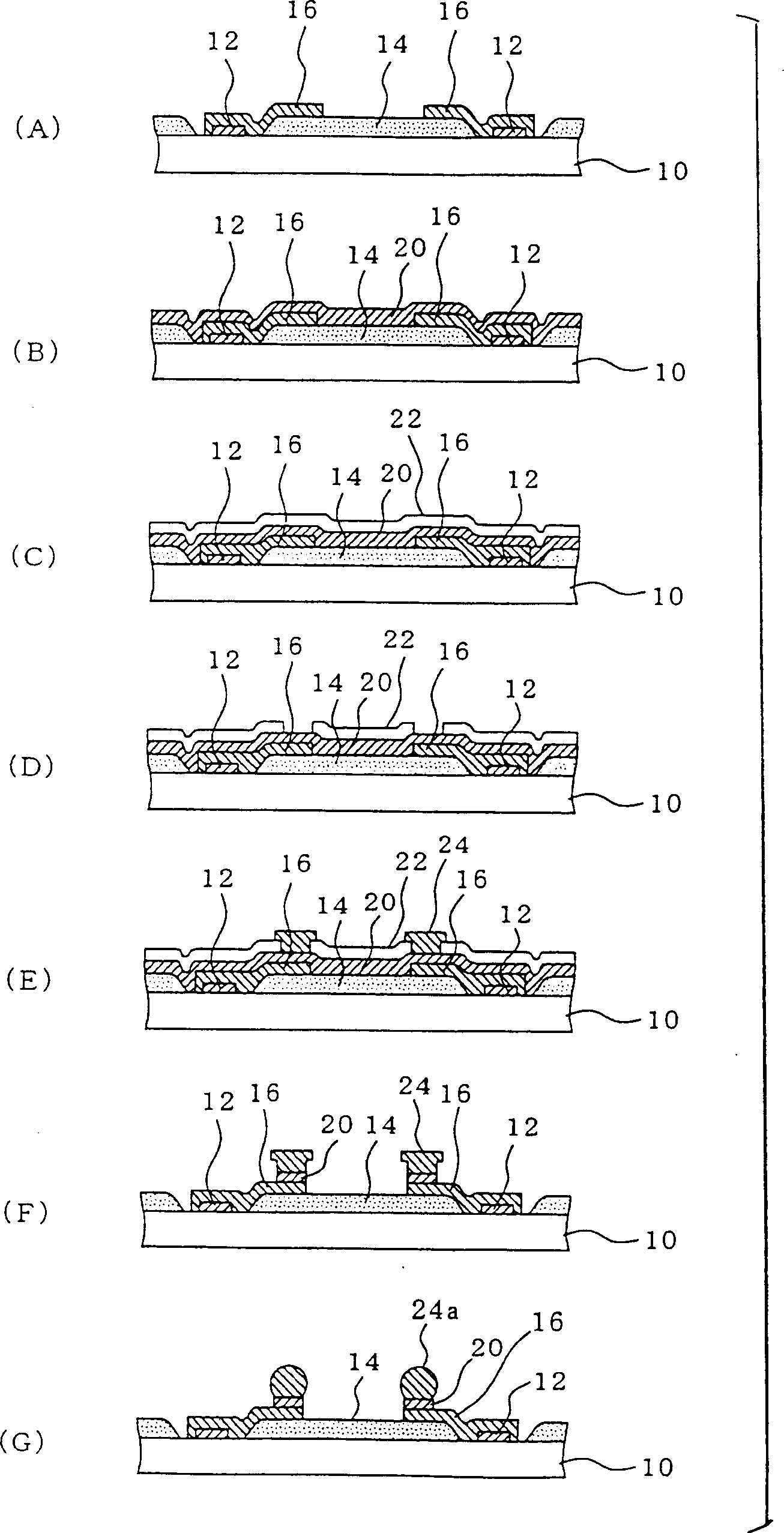
[0076] In the first embodiment and the second embodiment described later, a capacitor is formed on a semiconductor device having a CSP structure produced by the premise technology.

[0077] Figure 5 It is an explanatory diagram of the manufacturing method of the semiconductor device of the first embodiment. In addition, the present embodiment 1 is also carried out in the same manner as the above-mentioned premise technique. figure 1 (A)~(E), figure 2 The process shown in (A). Therefore, below, detailed explanations about the same steps as those of the above-mentioned premise technology will be omitted, and the parts different from the premise technology of the present embodiment 1 will be mainly described hereafter.

[0078] Such as Figure 5 As shown in (A), after forming the wiring 3 as a wiring layer on the chromium (Cr) layer 16 , the insulating layer 102 is formed on the entire surface of the wafer 10 . Here, the insulating layer 102 is made of photosensitive polyi...

Embodiment 2

[0093] Figure 7 It is an explanatory drawing of the manufacturing method of the semiconductor device of Example 2. In addition, since the second embodiment and the above-mentioned embodiment 1 Figure 5 The steps after the step shown in (C) to the sintering of the dielectric layer 104 are the same, so the difference between the second embodiment and the first embodiment will be mainly described here.

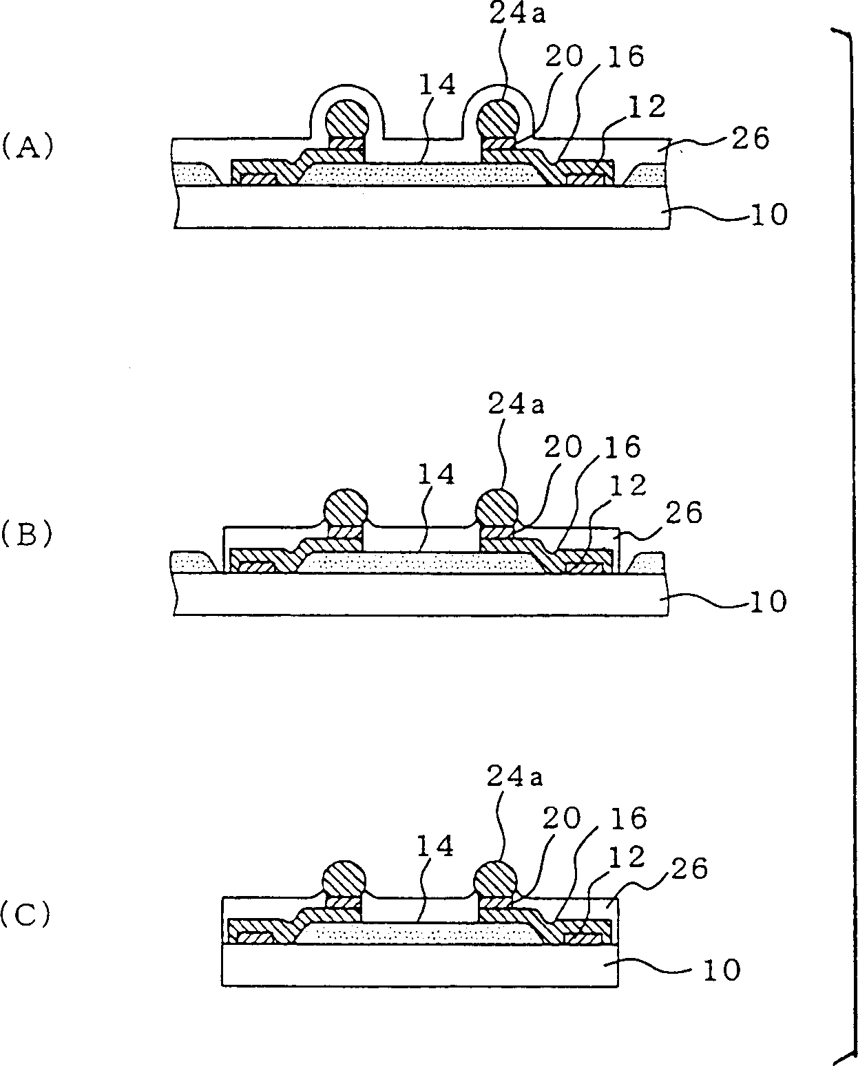
[0094] Such as Figure 7 As shown in (A), in the second embodiment, the conductive layer 112 is formed on the sintered dielectric layer 104 by applying a conductive liquid from the discharge head 101 . Since the conductive layer 112 corresponds to the copper (Cu) layer 20 of the above-mentioned premise technology, it may be formed of nickel (Ni) in addition to copper (Cu). In addition, support balls 24 a serving as external electrodes are formed on the conductive layer 112 as described in the aforementioned premise technique. After the supporting balls 24 a are formed, they...

Embodiment 3

[0100] In the third embodiment, an inductor is formed on a semiconductor device having a CSP structure formed according to the above-mentioned premise technique.

[0101] Figure 9 It is an explanatory drawing of the manufacturing method of the semiconductor device of Example 3. Figure 10 is through Figure 9 A plan view of a semiconductor device formed by the fabrication method shown. Figure 9 The manufacturing process shown is equivalent to Figure 10 The A-A cross-section has been fabricated.

[0102] In this embodiment 3, it is carried out in the same manner as the above-mentioned premise technology figure 1 (A)~(E), figure 2 The process shown in (A). Therefore, below, the detailed description of the same steps as those of the above-mentioned premise technology will be omitted, and the parts different from the premise technology of this embodiment 3 will be mainly described thereafter.

[0103] After forming the wiring 3 as a wiring layer on the chromium (Cr) lay...


PUM


Abstract

A method for manufacturing a semiconductor device includes the steps of forming a stress relief layer on a wafer such that the stress relief layer is away from at least part of electrodes formed on the wafer; forming a wiring layer in which lines that extend from the electrodes to the stress relief layer are formed; forming outer electrodes that are over the stress relief layer and are connected to the lines in the wiring layer; and forming a dielectric layer by applying dielectric liquid by an inkjet method to portions in the lines where the outer electrodes are connected to form a capacitor. The step of forming the dielectric layer is conducted after the step of forming the wiring layer.

Description

technical field [0001] The present invention relates to a method of manufacturing a semiconductor device having a CSP (chip scale package) structure and the semiconductor device. Background technique [0002] If high-density mounting of semiconductor devices is pursued, bare chip mounting is ideal. However, bare chips are difficult to guarantee quality and difficult to handle. Therefore, a package CSP (chip scale package) close to the size of a chip has been developed. In recent years, due to the demand for more compact electronic equipment, higher density mounting has been demanded, and a technology has been developed in which passive components mounted around the CSP are built into the CSP on the substrate and then packaged. For example, as a technique for embedding a capacitor in a CSP, there is a method of manufacturing a semiconductor device having a semiconductor substrate on which a circuit element formation region and a plurality of connection pads are formed, and ...

Claims


Application Information

Patent Timeline
Patent Type & Authority Applications(China)
IPC IPC(8): H01L23/52H01L21/3205H01L21/60H01L21/768H01L21/822H01L23/12H01L23/31H01L23/485H01L23/522H01L25/00H01L27/04
CPCH01L2924/01002H01L21/32051H01L2924/01047H01L2924/01004H01L2924/01006H01L2924/01078H01L2924/19041H01L2924/3011H01L24/11H01L2924/01079H01L2924/01074H01L23/5227H01L2924/01024H01L23/3114H01L2924/01005H01L2224/11334H01L2924/01082H01L2924/01057H01L2224/13099H01L2924/19042H01L2924/01056H01L2924/01013H01L2924/01022H01L24/12H01L2924/01003H01L2924/30107H01L2924/014H01L2924/01023H01L2924/01029H01L2924/30105H01L21/76804H01L2224/0231H01L2924/01033H01L2224/0401H01L2924/12042H01L2224/10126H01L2224/13022H01L2924/00
Inventor 村田昭浩
Owner SEIKO EPSON CORP
Why Eureka
Try Eureka