Driving circuit for display device

A technology of drive circuit and differential circuit, which is applied in the direction of electrical components, electronic switches, static indicators, etc.

Inactive Publication Date: 2004-08-18
RENESAS ELECTRONICS CORP
View PDF3 Cites 10 Cited by
  • Summary
  • Abstract
  • Description
  • Claims
  • Application Information

AI Technical Summary

Problems solved by technology

In this way, the differential amplifier circuit shown in Fig. 15 cannot be driven correctly (with high precision) in

Method used


Image

  • Driving circuit for display device
  • Driving circuit for display device
  • Driving circuit for display device

Examples


Embodiment

[0095] Embodiments of the present invention described above will be described in more detail, and embodiments of the present invention will be described here with reference to the accompanying drawings.

no. 1 example

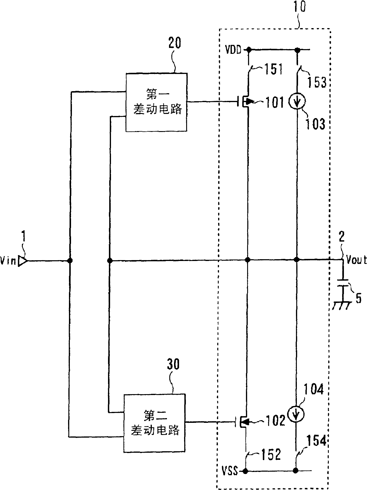
[0097] 4 is a schematic diagram showing the configuration of the drive circuit according to the first embodiment of the present invention, and is a schematic diagram showing specific examples of the first differential circuit 20 and the second differential circuit 30 in the first drive circuit. Next, configurations of the first and second differential circuits 20 and 30 will be described. The first differential circuit 20 includes: n-channel differential pair transistors 203, 204 driven by a constant current source 209; Transistors 201, 202 form a current mirror circuit. More specifically, one end of the constant current source 209 is connected to the low-potential power supply VSS, and the other end is connected to interconnected sources of the n-channel transistors 203, 204 constituting a differential pair. The current mirror circuit is composed of p-channel transistors 201 and 202, each source of which is connected to the high potential power supply VDD, the p-channel tran...

no. 2 example

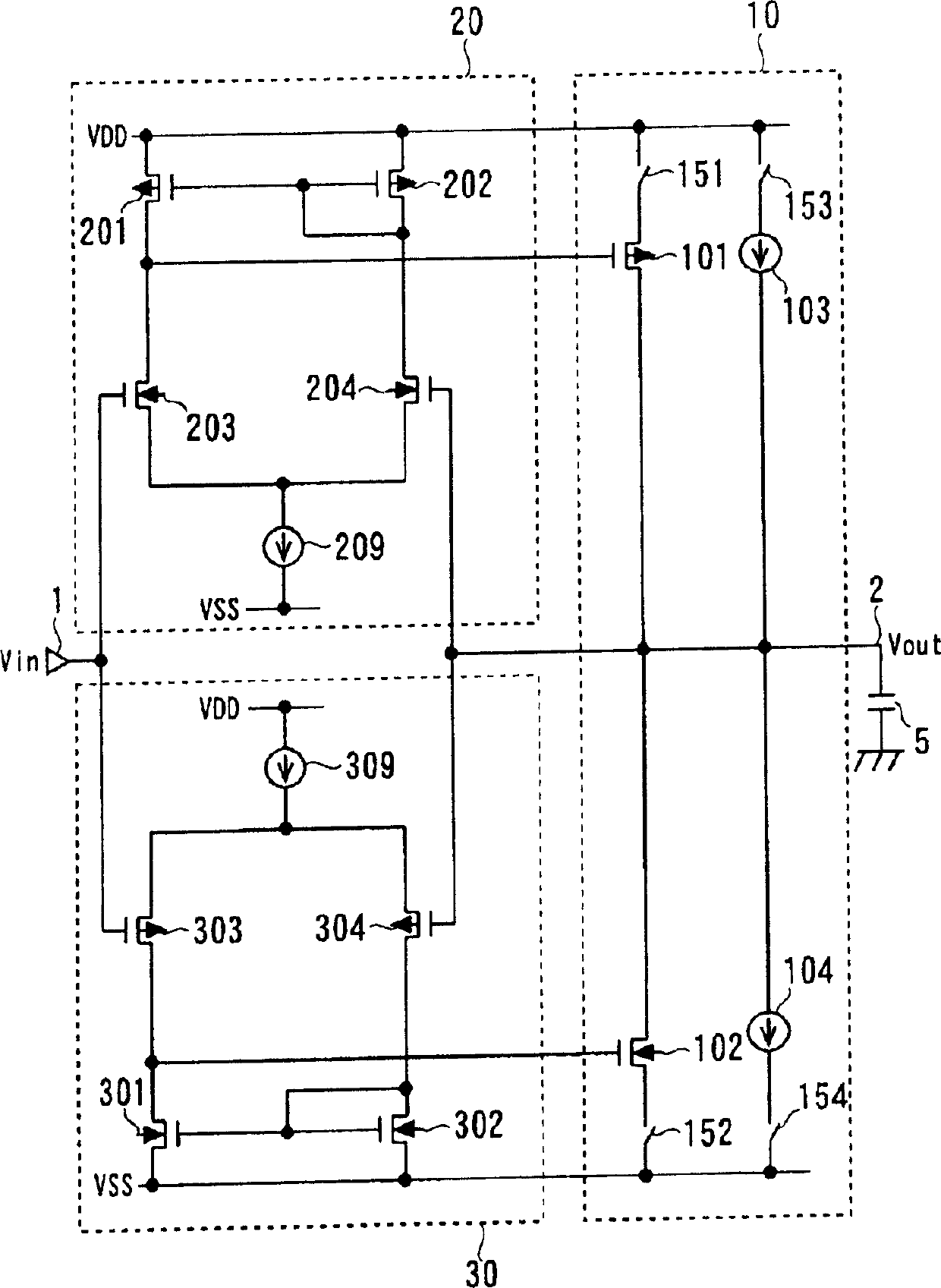
[0184]FIG. 7 shows the configuration of the drive circuit according to the second embodiment of the present invention, and shows an example of the configuration of the first and second differential circuits 20 and 30 of the drive circuit in FIG. 1 which is different from that in FIG. 4 . Next, configurations of the first and second differential circuits 20 and 30 will be described with reference to FIG. 7 . The structures of the first and second differential circuits 20, 30 on the inverting input side of the differential pair are different from those shown in FIG. 4 . Referring to Fig. 7, the first differential circuit 20 comprises n-channel differential pair transistors 203, 204, 205 driven by a constant current source 209; A current mirror circuit composed of p-channel transistors 201, 202. More specifically, one end of the constant current source 209 is connected to the low potential power supply VSS, and the other end is connected to the interconnected sources of the n-ch...


PUM


Abstract

Disclosed is a driving circuit for driving a capacitive load promptly to a target voltage. A first period and a second period are provided in one data driving period. During the first period, a transistor amplifier for driving the load for charging, with a setting drive voltage (V1), and a transistor amplifier for driving the load for discharging, with a setting drive voltage (V2), with V1 G09G 3/20 H03F 3/45 16 30 10 2004/2/12 1521714 2004/8/18 100495491 2009/6/3 2009/6/3 2009/6/3 Nippon Electric Co. Japan Tsuchi Hiroshi li xianglan 11021 The Patent Agency of the Chinese Academy of Sciences Inside the Chinese Academy of Sciences, No.52 Sanlihe Road, Fuwai, Beijing 100864 Japan 2003/2/12 2003-034130

Description

technical field [0001] The present invention relates to a driving circuit that drives a capacitive load to a required voltage within a given driving time, and particularly relates to the driver (buffer) portion of the output stage of a driving circuit suitable for a display device using an active matrix driving method Drive circuit. Background technique [0002] In recent years, with the development of information communication technology, the demand for portable devices having a display portion, such as mobile phones and portable information terminals, has increased. It is important for a portable device to be used continuously for a long time, and liquid crystal display devices are widely used as display parts of portable devices because of their low power consumption. Liquid crystal display devices have conventionally been transmissive with backlights, but reflective displays that use external light without backlights have been developed in order to achieve lower power c...

Claims


Application Information

Patent Timeline
IPC IPC(8): G02F1/133G09G3/20G09G3/36H03K17/687
CPCG09G2330/021G09G3/3688
Inventor 土弘
Owner RENESAS ELECTRONICS CORP
Why Eureka
Try Eureka