Great power MOSFET device and its manufacture
A technology of oxide semiconductor and field effect transistor, which is applied in the field of double-ditch gate power metal oxide semiconductor field effect transistor device, which can solve unevenness, prevent rapid current reverse and avalanche breakdown without any improvement, and current channel Stenosis and other problems
- Summary
- Abstract
- Description
- Claims
- Application Information
AI Technical Summary
Problems solved by technology
Method used
Image

Examples
Embodiment Construction
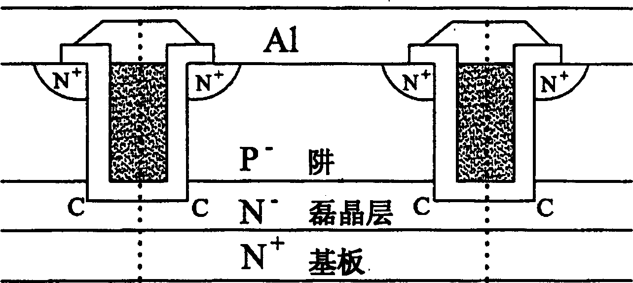
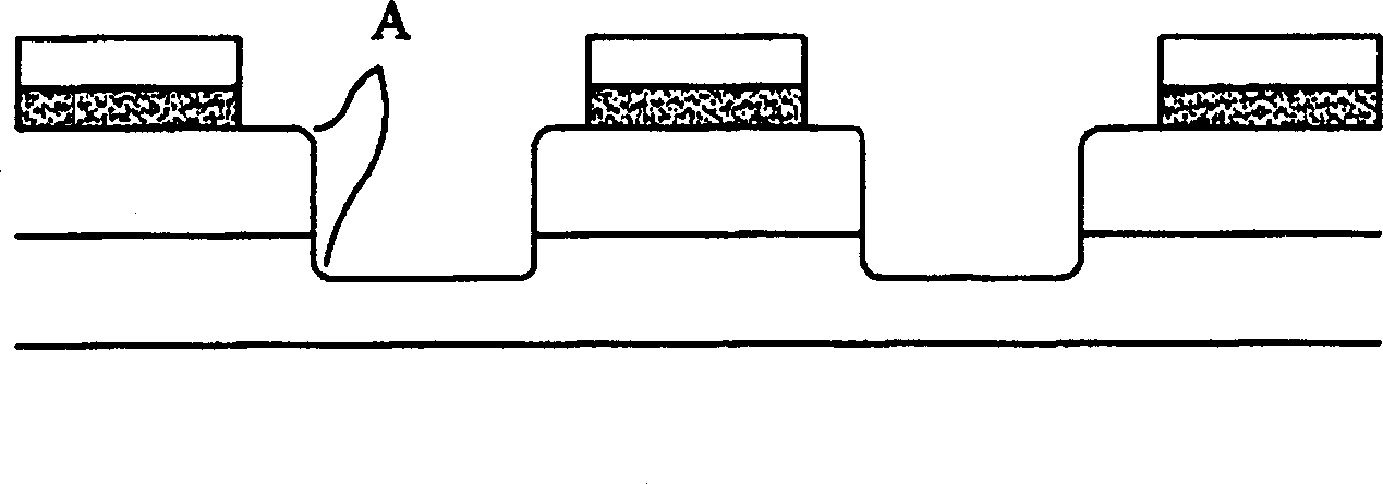
[0017] like Figure 3a to Figure 3g Shown in is the manufacturing steps of the embodiment of the self-aligned trench power metal-oxide-semiconductor field-effect transistor device of the present invention, wherein the N-channel type will be taken as an example for illustration, and the same component symbols will represent the same components.
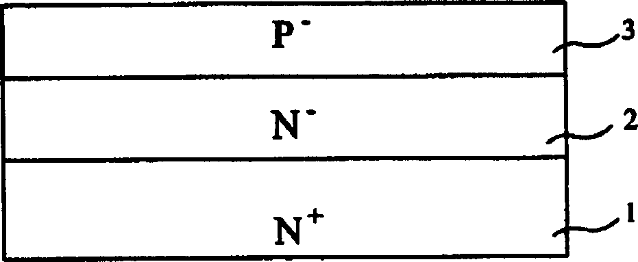
[0018] like Figure 3a shown in, providing a N + The first conductive type heavily doped silicon substrate 1, the silicon substrate 1 is used as the drain of the power MOSFET device, and a conductive metal can be plated on the lower surface as the drain contact (not shown). First, on the substrate 1 An epitaxial layer 2 is epitaxially formed, and then, a first conductivity type micro-dopant ion is implanted to form N - epitaxial layer 2, followed by the N - A well layer 3 is grown on the epitaxial layer, and the well layer 3 is implanted with a micro-dopant of the second conductivity type (P - ) formed; in Figure 3b In, a source ...
PUM
 Abstract
Description
Claims
Application Information
 - R&D
- Intellectual Property
- Life Sciences
- Materials
- Tech Scout
- Unparalleled Data Quality
- Higher Quality Content
- 60% Fewer Hallucinations
Browse by: Latest US Patents, China's latest patents, Technical Efficacy Thesaurus, Application Domain, Technology Topic, Popular Technical Reports.
© 2025 PatSnap. All rights reserved.Legal|Privacy policy|Modern Slavery Act Transparency Statement|Sitemap|About US| Contact US: help@patsnap.com