Semiconductor sensor for diameter of pore of human body

A semiconductor and biological technology, which is applied in the field of biological pore aperture semiconductor sensors, can solve the problem of not referring to the sensor, etc.

Inactive Publication Date: 2004-10-20
刘自鸿
View PDF0 Cites 3 Cited by
  • Summary
  • Abstract
  • Description
  • Claims
  • Application Information

AI Technical Summary

Problems solved by technology

After searching, no sensor that can reflect the change of pore diameter has been found in the literature at home and abroad.

Method used


Image

  • Semiconductor sensor for diameter of pore of human body
  • Semiconductor sensor for diameter of pore of human body
  • Semiconductor sensor for diameter of pore of human body

Examples


Embodiment Construction

[0017] The specific embodiment of the present invention will be described with reference to the accompanying drawings.

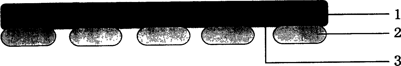
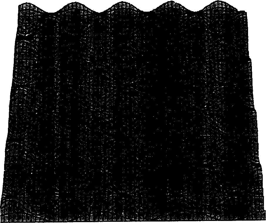
[0018] The shape and size of the sensor proposed by the present invention have no special regulations, but it is better to make the semiconductor sheet cover as many pores as possible. If a semiconductor sheet with a regular shape is used, it is beneficial to determine the functional relationship between the output voltage and the change of the pore diameter for future practical application. For example, when a rectangular semiconductor silicon wafer is used in the embodiment of the present invention, a Gaussian function relationship can be detected. The semiconductor material used in the present invention includes commonly used materials such as silicon, germanium, gallium arsenide, etc., and the doped impurities include commonly used boron, phosphorus, etc.

[0019] The present invention is described by taking a rectangular semiconductor silicon wafer as ...


PUM


Abstract

A semiconductor sensor for sensing the variation of the diameter of pore on human body is a doped semiconductor chip able to be pasted on the skin of human body. When it is serially connected in a DC loop with a constant-current source, its two power supply inputs are just the signal outputs. If said loop has a constant-voltage source, the current flowing through said loop is the output signal to be detected.

Description

technical field [0001] The invention relates to a biological pore aperture semiconductor sensor, which belongs to the technical field of semiconductor intelligent sensor design of bioelectronics. Background technique [0002] Pore ​​diameter is an important information window of human physiological changes. It can not only be used as an appearance parameter, but also reflect the suitability of cold and heat inside the human body, the degree of metabolism, and even the development of some diseases. After searching, no sensor that can reflect the change of pore diameter has been found in the literature at home and abroad. Contents of the invention [0003] The object of the present invention is to propose a semiconductor sensor capable of effectively responding to changes in the pore diameter of organisms including the human body. The sensor uses a semiconductor chip to sense array pores, and converts the radial displacement of the pores into electrical signal sensing output...

Claims


Application Information

Patent Timeline
Patent Type & Authority Applications(China)
IPC IPC(8): A61B5/00H01L35/00H01L49/00
Inventor 刘自鸿
Owner 刘自鸿
Why Eureka
Try Eureka