Micropattern forming material and fine structure forming method

A micro-pattern and micro-structure technology, which is applied in photosensitive material processing, photoplate-making process on patterned surface, photosensitive material used in photomechanical equipment, etc., can solve the problem of low reactivity, deformation of first resist pattern, formation Membrane reduction and other problems

Inactive Publication Date: 2004-12-29
RENESAS TECH CORP
View PDF3 Cites 5 Cited by
  • Summary
  • Abstract
  • Description
  • Claims
  • Application Information

AI Technical Summary

Problems solved by technology

[0012] However, in the method of forming a fine pattern by mutual diffusion of the resin components of the first resist and the second resist, the second resist is used in an organic solvent capable of dissolving the first resist. Soluble photoresist material, so there is a problem of deforming the first resist pattern
[0013] In addition, in the method of forming a fine pattern by forming a layer composed of a fine pattern forming material on a resist pattern, the reactivity of the fine pattern forming material to an acrylic resist etc. The film-forming property of the fine pattern forming material on the surface is lowered, and there is a problem that it is difficult to form a fine pattern with a desired size.
For example, when an ArF resist is used on a substrate, there is a problem that a layer composed of a fine pattern forming material can only be formed with a film thickness thinner than desired
[0014] In addition, when forming a fine pattern on a resist pattern, there is also a problem that defects such as bridging (bridging) that are partially connected to each other occur between the patterns.

Method used


Image

  • Micropattern forming material and fine structure forming method
  • Micropattern forming material and fine structure forming method
  • Micropattern forming material and fine structure forming method

Examples


Embodiment approach 1

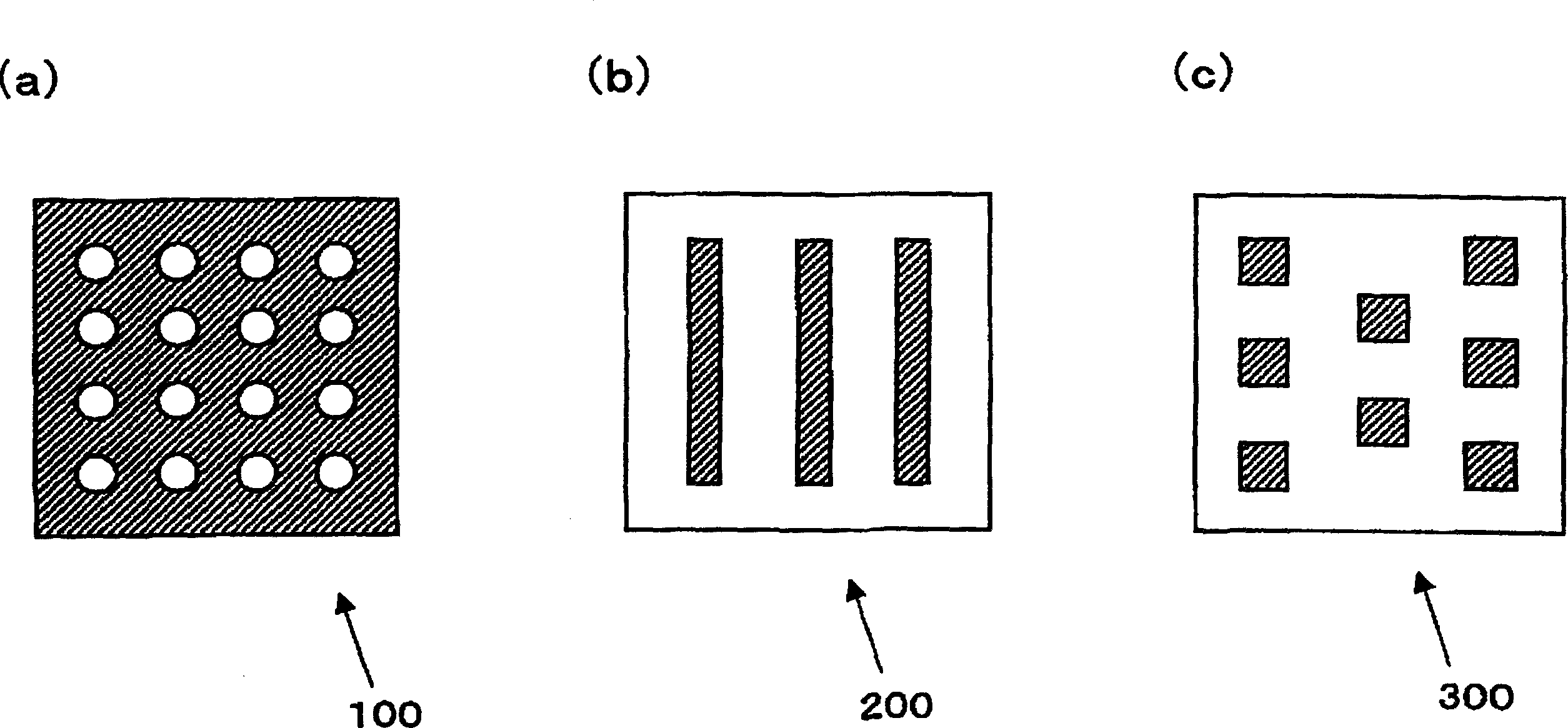
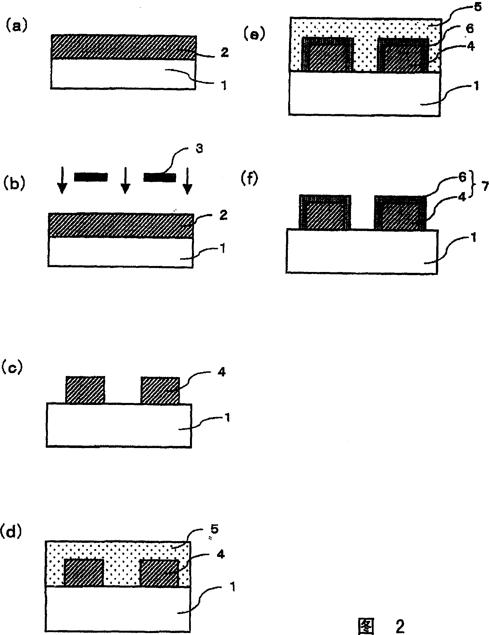
[0044] figure 1 It is a diagram showing an example of a mask pattern for forming a resist pattern finely divided as a target in the present invention. figure 1 (a) is a masking pattern 100 of fine holes, figure 1 (b) is a mask pattern 200 at fine intervals, figure 1 (c) is the pattern 300 left in isolation. In the figure, for example, hatched portions indicate resist-formed portions. In addition, FIG. 2 is a process diagram showing an example of the semiconductor device manufacturing method according to the present embodiment.

[0045] First, as shown in FIG. 2( a ), a resist composition is applied on a semiconductor substrate 1 to form a resist film 2 . For example, a resist composition having a film thickness of about 0.7 μm to 1.0 μm is applied on a semiconductor substrate by using a spin coating method or the like.

[0046] In this embodiment, as a resist composition, a resist that generates an acid component inside the resist by heating is used. Examples of the resi...

Embodiment approach 2

[0141] In this embodiment, it is characterized in that exposure is performed before the MB processing described in Embodiment 1.

[0142] Figure 4 is a process diagram showing an example of a method of manufacturing a semiconductor device according to this embodiment. Figure 4 (a)-(d) are carried out according to the same process as Fig. 2(a)-(d). That is, after the resist composition is coated on the semiconductor substrate 8 to form the resist film 9, exposure is performed through the mask 10 to form the resist pattern 11. Here, as the resist composition in this embodiment, a chemically amplified resist that generates oxygen by exposure can be used.

[0143] Then, form as Figure 4 After forming the film 12 with the fine pattern shown in (d), as Figure 4 As shown in (e), the entire surface of the semiconductor substrate 8 is exposed using g-rays or i-rays from a mercury lamp. Thereby, instead of the MB treatment or before the MB treatment, acid can be generated in th...

Embodiment approach 3

[0157] In this embodiment mode, it is characterized in that only a desired region of the semiconductor substrate is exposed after forming a resist pattern.

[0158] Figure 5 is a process diagram showing an example of a method of manufacturing a semiconductor device according to this embodiment. Figure 5 (a)-(d) are carried out according to the same process as Fig. 2(a)-(d). That is, after the resist composition is coated on the semiconductor substrate 15 to form the resist film 16, exposure is performed through the mask 17 to form the resist pattern 18. Here, as the resist composition in this embodiment, a chemically amplified resist that generates acid by exposure can be used.

[0159] Then, form as Figure 5 (d) After forming the film 20 with a fine pattern shown in (d), to Figure 5 As shown in (e), the resist pattern is selectively exposed using a suitable light shield 19 . For exposure, for example, g-rays or i-rays from a mercury lamp can be used. Thus, acid can ...


PUM

PropertyMeasurementUnit
thicknessaaaaaaaaaa

Abstract

The fine pattern forming material comprises a water-soluble component which is cross-linkable by the presence of an acid, and water and / or a water-soluble organic solvent, wherein the water-soluble component is at least one selected from the group consisting of a water-soluble polymer, a water-soluble monomer, a water-soluble oligomer, a copolymer of a water-soluble monomer and salts of these. The fine pattern forming material is formed on a resist pattern 4 capable of supplying the acid and the water-soluble component causes a cross-linking reaction under the acid from the resist pattern 4 in parts in contact with the resist pattern 4 to form a water-or alkali-insoluble film 6.

Description

technical field [0001] The present invention relates to a fine pattern forming material and a method for forming a fine structure. Background technique [0002] In recent years, along with the increase in the degree of integration of semiconductor devices, the size of each element has been miniaturized, and the width of wirings, gate electrodes, etc. constituting each element has also been miniaturized. Generally, after forming a desired resist pattern using photolithography, fine patterns are formed by etching various thin films of the substrate using the resist pattern as a mask. For this reason, photolithography is very important in forming fine patterns. [0003] Photolithography consists of the processes of resist coating, mask alignment, exposure and development. However, in recent cutting-edge devices, the pattern size is approaching the limit resolution of photoexposure, so development of exposure technology with higher resolution is required. [0004] As a conven...

Claims


Application Information

Patent Timeline
Patent Type & Authority Applications(China)
IPC IPC(8): H01L21/027G03F7/20G03F7/40H01L21/312
CPCG03F7/2024G03F7/40H01L21/312H01L21/02118H01L21/02282H01L21/027
Inventor 寺井护丰岛利之石桥健夫樽谷晋司
Owner RENESAS TECH CORP
Why Eureka
Try Eureka