
Method and structure for forming barrier layer

A barrier layer and object layer technology, applied in the direction of electrical components, semiconductor/solid-state device manufacturing, circuits, etc., can solve problems such as damaging semiconductor components, affecting the electrical properties of the dielectric layer, and reducing the resistivity of the barrier layer 190

Inactive Publication Date: 2005-01-19
UNITED MICROELECTRONICS CORP
View PDF3 Cites 14 Cited by
  • Summary
  • Abstract
  • Description
  • Claims
  • Application Information

AI Technical Summary

Problems solved by technology

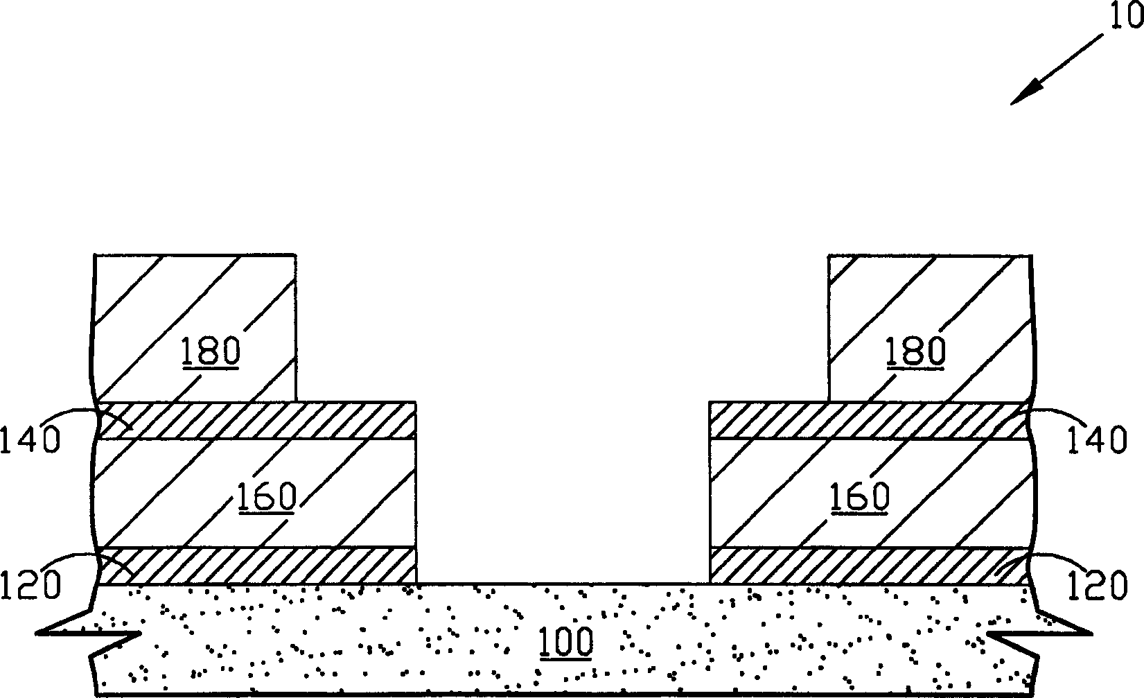
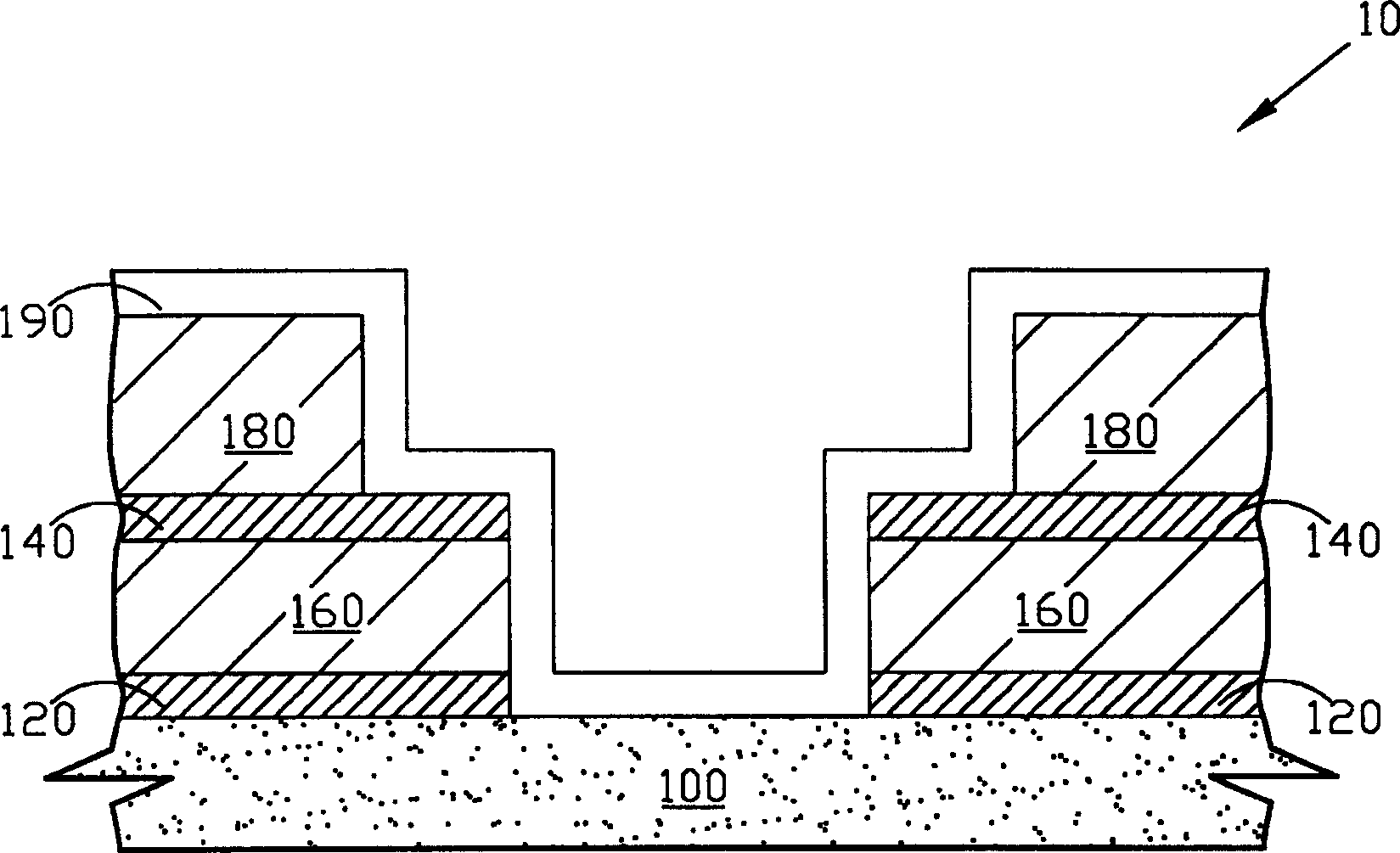
[0004] In the prior art, in order to prevent copper metal atoms from diffusing into the dielectric layer, such as titanium nitride (TiN) or tantalum nitride (TaN) is usually used to make the barrier layer, US Patent No. US 6,541,374 B1 is It is mentioned that TiN is used to form the barrier layer, but actually when the barrier layer 190 is deposited, since the deposition direction is approximately perpendicular to the wafer surface, the thickness deposited on the sidewall of the dual damascene structure 10 will be approximately Only one-fifth to one-half of the thickness deposited above the bottom of the hole in the first dielectric layer 160 and the bottom of the trench in the second dielectric layer 180 is likely to cause incomplete sidewall deposition and make the rear dual damascene structure 10 The copper metal atoms formed in the dielectric layer diffuse into the dielectric layer, thereby affecting the electrical properties of the dielectric layer and damaging the entire semiconductor device. Therefore, the barrier layer on the inner wall of the dual damascene structure 10 is completely deposited to prevent the diffusion of copper metal atoms. to the requirement within the dielectric layer
[0005] On the other hand, the resistivity of metal nitride in the prior art is much higher than that of metal materials, so when titanium nitride or tantalum nitride is used as the barrier layer 190 in the dual damascene structure 10, it will make The resistivity between metals in the dual damascene structure 10 is too high to affect the operating speed and power consumption of the semiconductor device, so there is a need to reduce the resistivity of the barrier layer 190 above the bottom of the hole in the first dielectric layer 160

Method used


Image

  • Method and structure for forming barrier layer
  • Method and structure for forming barrier layer
  • Method and structure for forming barrier layer

Examples


Embodiment Construction

[0015] Some embodiments of the present invention are described in detail as follows. However, the invention can be broadly practiced in other embodiments than those described in detail. That is, the scope of the present invention is not limited by the proposed embodiments, but should be defined by the scope defined in the following claims.

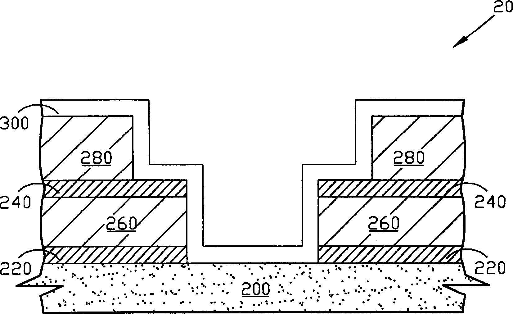
[0016] In the first embodiment of the present invention, as Figure 2A As shown in ~E, a dual damascene structure 20 has been formed above a metal layer 200 of a wafer. This dual damascene structure 20 is composed of a first etch stop layer 220, a first dielectric layer 260 above the first etch stop layer 220, The second etch stop layer 240 above the first dielectric layer 260 and the second dielectric layer 280 above the second etch stop layer 240 are formed, wherein the metal layer 200 is a copper metal layer, and the first etch stop layer 220 The material of the second etch stop layer 240 is to prevent copper metal atoms from diffusin...


PUM


Abstract

The invention is a method of forming blocking layer, firstly making a double inserted structure on a metallic layer, where the structure contains a first dielectric layer and a second one, the former containing a hole and the latter containing a groove, successively forming a first tantalum metal layer on the structure, then forming a tantalum nitride layer on the first tantalum metal layer, eliminating the tantalum metal layer above the bottom of the hole in the first dielectric layer in an ion spattering mode, where the tantalum atoms in the eliminated tantalum nitride layer will deposit on the side wall of the hole in the first dielectric layer, and finally forming a second tantalum metal layer on the remained tantalum nitride layer, where there are only the first and second tantalum metal layers above the bottom of the hole, and the made blocking layer will have lower resistivity at the bottom of the hole and an ability to completely block copper atoms from diffusing to the dielectric layer.

Description

(1) Technical field [0001] The present invention is a semiconductor manufacturing method, especially a method of manufacturing an internal barrier layer of a damascene structure. (2) Background technology [0002] In the semiconductor manufacturing process, after the active components of the semiconductor components above the substrate are fabricated, the next step is to fabricate the metal wires above the active components of the completed semiconductor components to complete the internal circuit connection of the semiconductor components to be fabricated. Wire. In the manufacturing process of the above-mentioned metal wires, a metal layer is usually first formed above the active element of the semiconductor element, and then the first layer of metal layer is completed by photoresist, lithography, and etching, and then the first layer of metal layer A layer of dielectric layer is deposited on the top, corresponding to the needs of different semiconductor components, and th...

Claims


Application Information

Patent Timeline
Patent Type & Authority Applications(China)
IPC IPC(8): H01L21/31H01L21/3205H01L21/768
Inventor 杨玉如黄建中
Owner UNITED MICROELECTRONICS CORP
Learn More