Liquid crystal display device

A technology of liquid crystal display and liquid crystal components, which is applied in the direction of static indicators, instruments, transistors, etc., and can solve problems such as inappropriate

Inactive Publication Date: 2005-02-09
SEMICON ENERGY LAB CO LTD
View PDF1 Cites 31 Cited by
  • Summary
  • Abstract
  • Description
  • Claims
  • Application Information

AI Technical Summary

Problems solved by technology

Therefore, the pixel part can be used as a switching element, but it is not suitable as a scanning line driver circuit for selecting pixels, or a signal line driver circuit for supplying video signals to the selected pixels, etc., which require high-speed operation.

Method used


Image

  • Liquid crystal display device
  • Liquid crystal display device
  • Liquid crystal display device

Examples


Embodiment 1

[0101] This embodiment will explain one mode of the semi-crystalline TFT possessed by the liquid crystal display device of the present invention.

[0102] Picture 11 A is a top view of the semi-crystalline TFT of this embodiment, Picture 11 B is along Picture 11 A-A' cut cross-sectional view in A. 1301 denotes a gate wiring part of which functions as a gate electrode, and a gate insulating film 1302 is interposed and overlapped with a first semiconductor film 1303 formed of a semi-crystalline semiconductor. In addition, second semiconductor films 1304a, 1304b functioning as LDD regions connected to the first semiconductor film 1303 are formed, and third semiconductor films 1305a, 1305b of one conductivity type connected to the second semiconductor films 1304a, 1304b are formed. In addition, 1306 and 1307 correspond to wirings connected to the third semiconductor films 1305a and 1305b.

[0103] in Picture 11 In the shown semi-crystalline TFT, a certain channel length can be mai...

Embodiment 2

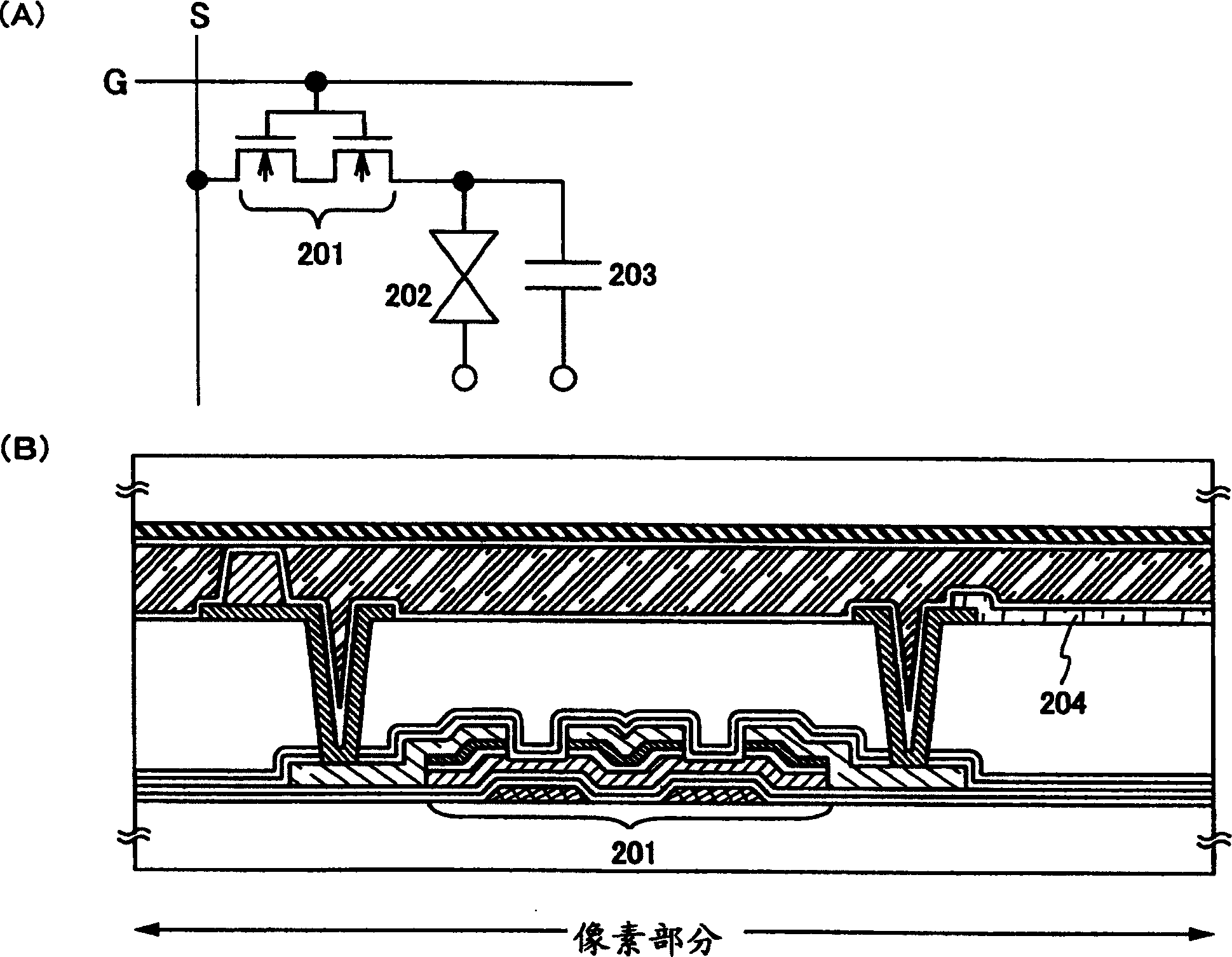
[0105] This embodiment will explain a mode of a shift register using semi-crystalline TFTs with all uniform polarities. Picture 12 A illustrates the structure of the shift register of this embodiment. Picture 12 The shift register shown in A uses the first clock signal CLK, the second clock signal CLKb, and the start pulse signal SP to operate. 1401 represents the pulse output circuit, and its specific structure is shown in Picture 12 In B.

[0106] The pulse output circuit 1401 includes TFTs 801-806 and a capacitive element 807. The gate of the TFT 801 is connected to node 2, the source is connected to the gate of the TFT 805, and the potential Vdd is supplied to the drain. The gate of the TFT 802 is connected to the gate of the TFT 806, the drain is connected to the gate of the TFT 805, and the potential Vss is supplied to the source. The gate of the TFT 803 is connected to node 3, the source is connected to the gate of the TFT 806, and the potential Vdd is supplied to the dr...

Embodiment 3

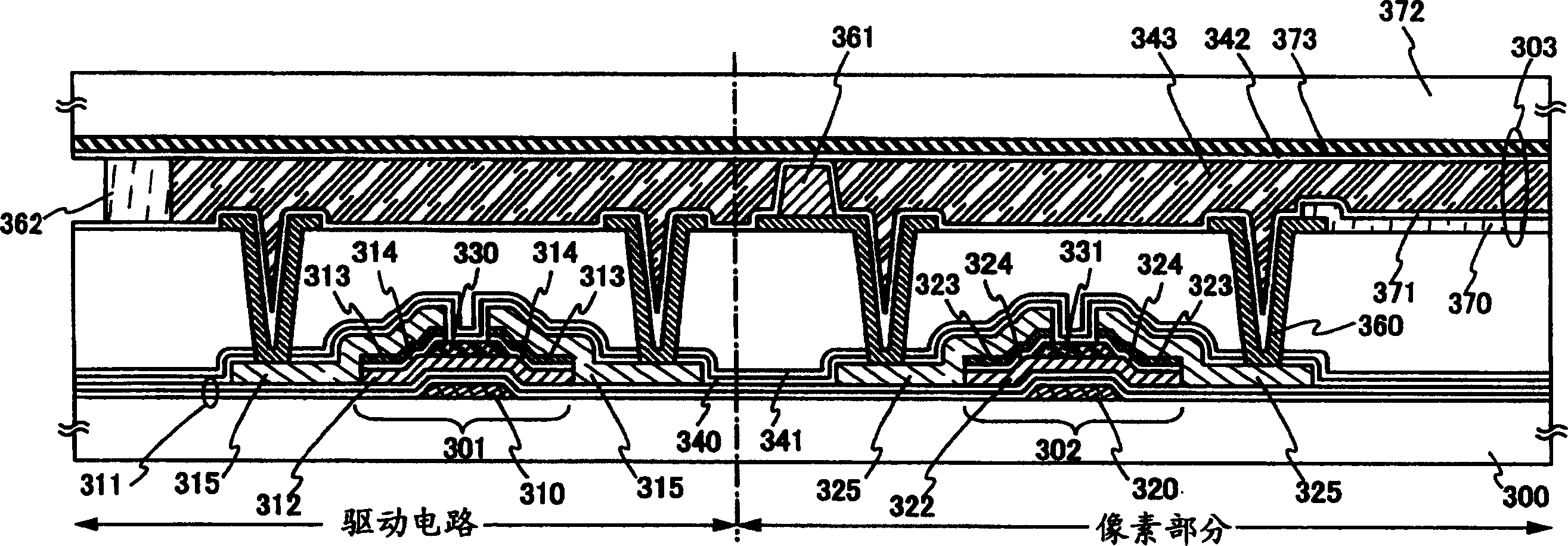
[0112] In this embodiment, use Figure 13 The appearance of a panel corresponding to one mode of the liquid crystal display device of the present invention will be described. Figure 13 A is a plan view of the panel, in which the semi-crystalline TFT 4010 and the liquid crystal element 4011 formed on the first substrate 4001 are sealed between the second substrate 4006 and the second substrate 4006 with a sealing material 4005. Figure 13 B is equivalent to along Figure 13 A-A' cut cross-sectional view in A.

[0113] A sealing material 4005 surrounding the pixel portion 4002 formed on the first substrate 4001 and the scanning line driving circuit 4004 is provided. A second substrate 4006 is provided over the pixel portion 4002 and the scan line driving circuit 4004. Therefore, the pixel portion 4002, the scan line driving circuit 4004, and the liquid crystal 4007 are sealed by the first substrate 4001, the sealing material 4005, and the second substrate 4006 together. In addition...


PUM


Abstract

Provided is a liquid crystal display device which is made in system-on-panel structure without complicating processes for TFTs and further can inhibit cost increase. The liquid crystal display is characterized in that: a pixel part is provided with a liquid crystal element and a pixel having a TFT controlling a voltage applied to the liquid crystal element; a TFT that a driving circuit has and the TFT controlling the voltage applied to the liquid crystal element have a gate electrode, a gate insulating film formed on the gate electrode, a 1st semiconductor film overlapping with the gate electrode across the gate insulating film, and a couple of 2nd semiconductor films formed on the 1st semiconductor film; impurities which impart a one-conductivity type are added to the couple of 2nd semiconductor films; and the 1st semiconductor film is formed of a semiamorphous semiconductor.

Description

Technical field [0001] The present invention relates to a liquid crystal display device that uses thin film transistors as its driving circuit and pixel parts. Background technique [0002] With the increase of the resolution of the liquid crystal display device formed with an inexpensive glass substrate, the area around the pixel portion for mounting (the frame area) occupies an increase in the substrate, which hinders the exquisiteness of the liquid crystal display device Tendency to change. Therefore, it can be considered that the method of mounting IC (integrated circuit) formed of a single crystal silicon wafer on a glass substrate has its limits. The technology in which the integrated circuit including the driving circuit and the pixel portion are integrally formed on the same glass substrate, which is the so-called system on panel, has attracted attention. [0003] The mobility of a thin film transistor (polycrystalline TFT) using a polycrystalline semiconductor film is 2 ...

Claims


Application Information

Patent Timeline
Patent Type & Authority Applications(China)
IPC IPC(8): G02F1/133G02F1/136H01L29/786
Inventor 山崎舜平
Owner SEMICON ENERGY LAB CO LTD
Why Eureka
Try Eureka