Test electrode for single unidimensional nano material and fabricating method thereof

A technology of nano-materials and test electrodes, which is applied in the analysis of materials, material analysis by electromagnetic means, and measurement devices, etc. It can solve the difficulties in making shape and size test electrodes, increase the production time and cost, and affect the measurement of electrical properties, etc. problems, to achieve the effect of precise production, increased flexibility and high precision

Inactive Publication Date: 2005-04-06
INST OF PHYSICS - CHINESE ACAD OF SCI
View PDF0 Cites 15 Cited by
  • Summary
  • Abstract
  • Description
  • Claims
  • Application Information

AI Technical Summary

Problems solved by technology

But the shortcomings are also obvious. On the one hand, a large number of electrodes are required on a substrate, which increases the production time and cost, and the contact resistance between the material and the electrodes is high, which affects the measurement of electrical properties; on the other hand, due to the one-dimensional The nanomaterials are randomly distributed on the substrate, the success rate is low, and this method is difficult to produce a single one-dimensional nanomaterial test electrode with special requirements for shape and size
[0005] Therefore, the application of the above two methods to make a test electrode of a single one-dimensional nanomaterial has great defects.

Method used


Image

  • Test electrode for single unidimensional nano material and fabricating method thereof
  • Test electrode for single unidimensional nano material and fabricating method thereof
  • Test electrode for single unidimensional nano material and fabricating method thereof

Examples


Embodiment 1

[0039] In this embodiment, a single one-dimensional Ag nanowire test electrode is produced, and the specific production steps are as follows:

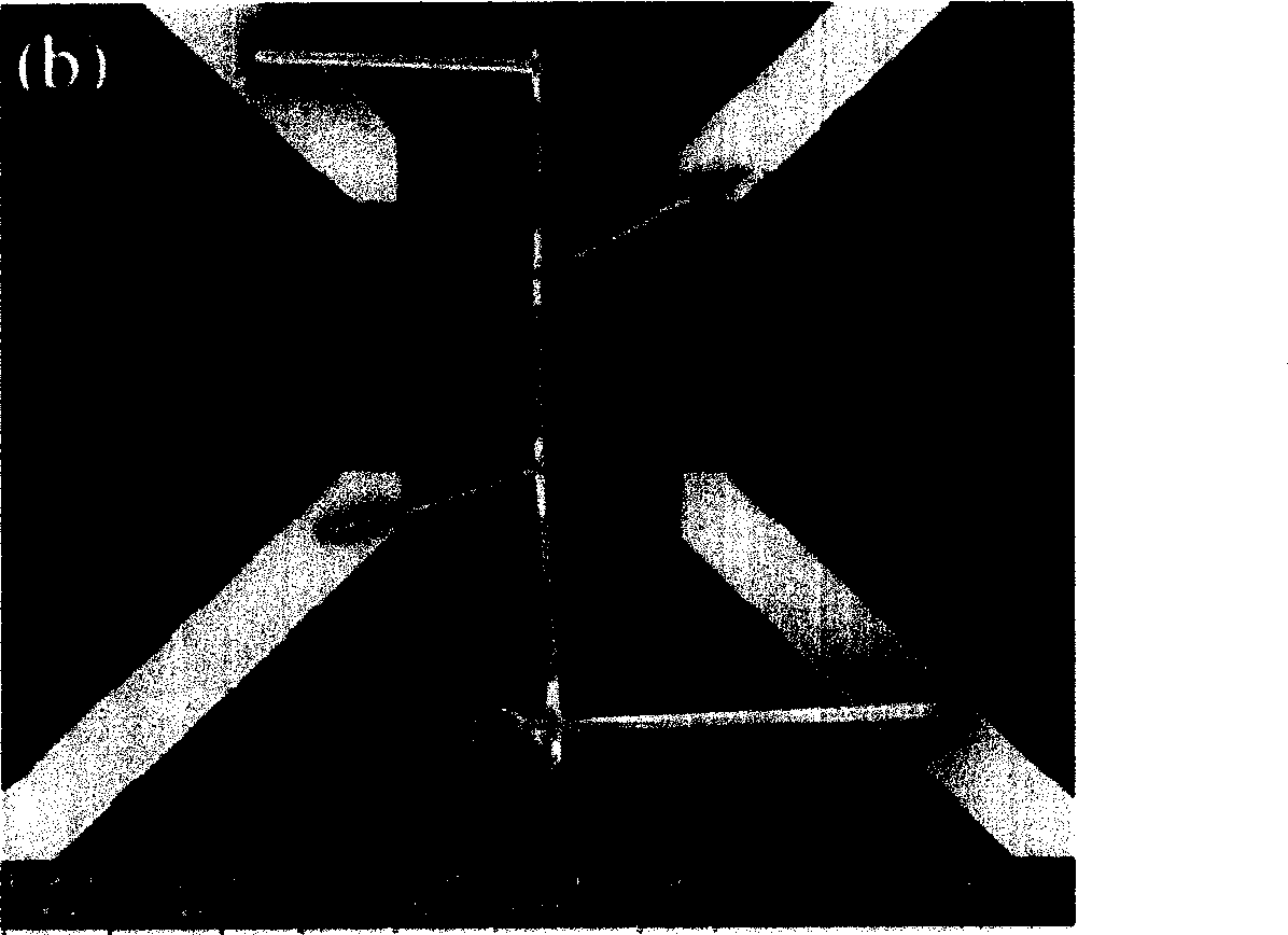
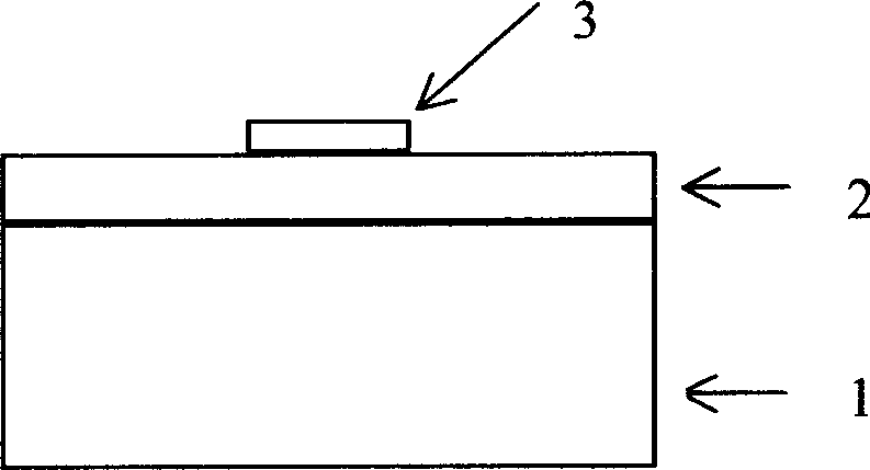
[0040] Such as figure 2 As shown, the substrate material 1 of the substrate is a Si sheet, on which a Si 3 N 4 The insulating layer 2, whose thickness is 200nm, will set Si 3 N 4 The substrate of the edge layer is put into the focused ion beam system, and at any place within the range of 1 mm to 1.5 mm from the four corners of the substrate, the T-shaped Pt mark is deposited by the focused ion beam system, with a size of 2×10 μ and a deposition height of about It is 200nm, the ion beam current is 100pA, and the deposition time is about 90 seconds. Sprinkle the dispersed Ag nanowires on the substrate by spin coating, put the substrate into the electron beam exposure system for calibration and read the coordinate values ​​(u1, v1) (u2, v2) at both ends of the Ag nanowires. Look for multiple nanowires on the same piece, but the dist...

Embodiment 2

[0042] The present embodiment makes one-dimensional T (or Y) type carbon nanotube test electrode, concrete steps are as follows:

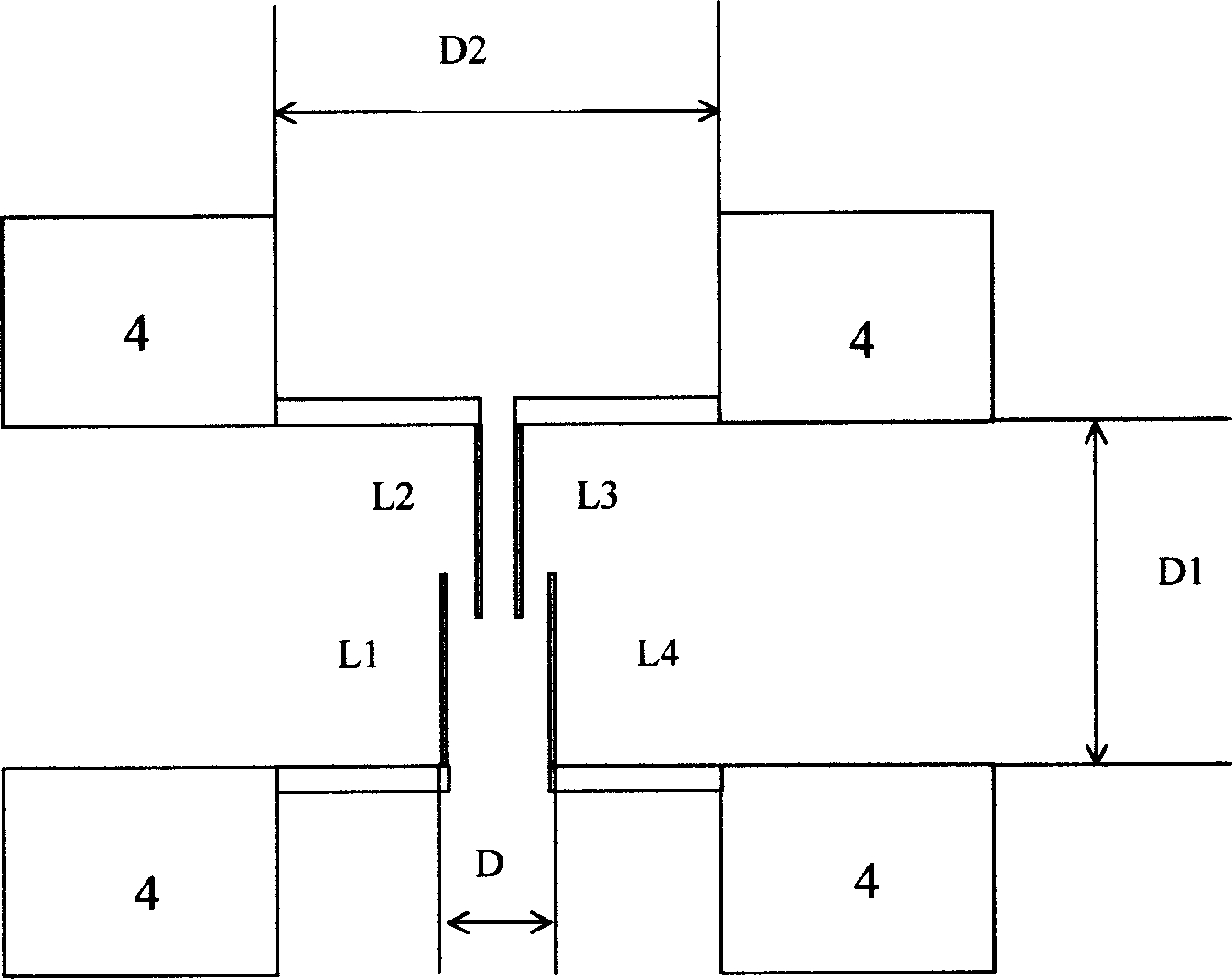
[0043] The substrate of the substrate is Si, and the insulating layer is SiO 2 , with a thickness of 400 nm. T (or Y) type carbon nanotubes are grown directly on the substrate. A focused ion beam system is used to etch a T-shaped mark with a size of 2×10μ, an etching height of about 200nm, an ion beam current of 200pA, and an etching time of about 60 seconds. Read the coordinates of the T (or Y) carbon nanotube node and the three endpoints. Design the electrode pattern according to the size of the T (or Y) tube. A 950PMMA electron beam resist is used, and the spin coating speed is 3000rpm. At this time, the thickness of the electron beam resist is about 260nm, and the pre-baking is performed on a hot plate at 180°C for 1 minute. Exposure parameters: write field size 100μm, accelerating voltage 10kV, aperture 30μm, working height 5mm, exposure d...

Embodiment 3

[0045] In this embodiment, a single one-dimensional boron nanowire test electrode is fabricated, and the specific steps are as follows:

[0046] The substrate of the substrate is Si, and the insulating layer is SiO 2 , with a thickness of 300 nm. Sprinkle the dispersed boron nanowires on the substrate by spin coating, and use the focused ion beam system to deposit T-shaped Pt marks with a size of 4×10μ and a deposition height of about 400nm. The ion beam current is 200pA, and the deposition time is about 100 seconds. Read the coordinate values ​​(u1, v1) (u2, v2) at both ends of the boron nanowire, and design the electrode pattern according to the size of the boron nanowire. ZEP520 electron beam resist was used, and the spin coating speed was 3000 rpm. At this time, the thickness of the electron beam resist was about 240 nm, and the pre-baking was performed on a hot plate at 200° C. for 2 minutes. Exposure parameters: write field size 200μm., accelerating voltage 30kV, aper...


PUM

PropertyMeasurementUnit
thicknessaaaaaaaaaa
thicknessaaaaaaaaaa
thicknessaaaaaaaaaa

Abstract

This invention discloses a single one-dimension nanometer test electrode and its process method. The electrode comprises the following: a underlay with its thickness at 0.5 to 2 mm; an isolation layer on the underlay with the single one-dimension nanometer material distributing on the isolation layer. The metal electrode comprises electrode wire contacted with the material and connection part as lead wire. This method realizes the single one-dimension nanometer material accurate position on the base plate by use of focus ion beam system with high-resolution rate.

Description

technical field [0001] The invention relates to a test electrode of a single one-dimensional nanometer material and a manufacturing method thereof. Background technique [0002] The characterization of the physical properties of one-dimensional nanomaterials has always been the focus of research, especially the measurement of the intrinsic physical properties of a single one-dimensional nanomaterial. The design and fabrication of the measurement electrode is the basis and key to achieve this purpose. There are two main methods of making electrodes: [0003] One is to directly use focused ion beam technology to make electrodes, as described in "Nanotechnology", 2002, Vol.13, No.5: 653-658 "Making electrical contacts to nanowires with a thick oxide layer" thick oxide coating) discloses this method, which uses a double-beam focused ion beam system, first uses electron beams to find the position of a single one-dimensional nanomaterial, then uses ion beams to locate, and then u...

Claims


Application Information

Patent Timeline
Patent Type & Authority Applications(China)
IPC IPC(8): G01N27/00
Inventor 杨海方刘立伟金爱子顾长志吕力
Owner INST OF PHYSICS - CHINESE ACAD OF SCI
Why Eureka
Try Eureka