
Selective etching of carbon-doped low-k dielectrics

A low dielectric constant material, selective technology, used in circuits, electrical components, semiconductor devices, etc.

Inactive Publication Date: 2005-06-08
APPLIED MATERIALS INC
View PDF2 Cites 10 Cited by
  • Summary
  • Abstract
  • Description
  • Claims
  • Application Information

AI Technical Summary

Problems solved by technology

[0005] Another problem in etching low-k materials is the etch rate of low-k materials due to the pattern density and the size of the etched feature pattern (via hole or channel), which is the etch rate microload ( microloading), or microloading

Method used


Image

  • Selective etching of carbon-doped low-k dielectrics
  • Selective etching of carbon-doped low-k dielectrics
  • Selective etching of carbon-doped low-k dielectrics

Examples


example

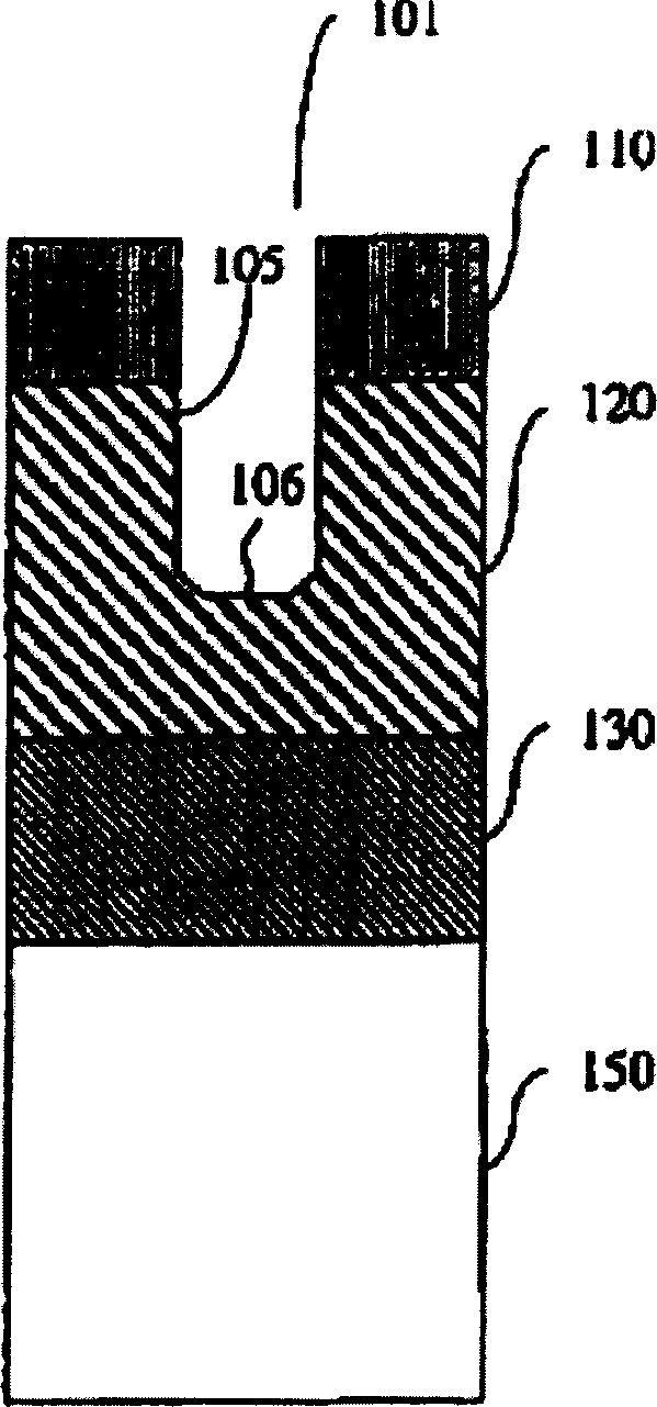
[0043] The following example describes the use of the method of the present invention to etch the low-k material layer 120 on the substrate 150 . An example of the substrate 150 is, for example, a silicon wafer with a diameter of 200 mm (8 inches) or 300 mm (12 inches). Such as figure 1 As shown, the wafer 150 is covered with a barrier / liner layer 130 with a thickness of hundreds of angstroms, a low dielectric constant material layer 120 with a thickness of 0.4-1.5 microns, and a mask layer 110 with a thickness of about 1930 angstroms. The mask layer 110 is patterned for etching a defined pattern of features 101 .

[0044] In the following examples, the mask layer is a photoresist such as "RISTON" manufactured by duPont de Nemours Chemical Company. The low dielectric constant material layer includes carbon-doped dielectric materials, such as organosilicate glass (OSG) doped with CH3, organic polymers (such as benzene cyclobutene, parylene, polytetrafluoroethylene, etc.) , p...


PUM

PropertyMeasurementUnit
thicknessaaaaaaaaaa
thicknessaaaaaaaaaa
diameteraaaaaaaaaa

Abstract

A plasma etch process for selectively etching low dielectric constant materials on a substrate in a plasma etch chamber. The process utilizes an etching gas mixture for etching, and the etching gas mixture includes a polyfluorinated fluorocarbon or hydrofluorocarbon gas, a nitrogen-containing gas, and one or more additive gases, such as a polyfluorinated A hydrofluorocarbon gas of hydrogen, an inert gas and / or a carbon-oxygen gas. When etching the low dielectric constant material layer with this process, the etching selectivity ratio of the low dielectric constant material layer and the photoresist mask is greater than about 5:1, and the etching selectivity ratio of the low dielectric constant material layer and the barrier / liner layer The ratio is greater than 10:1, and the etch rate of the low dielectric constant material layer is greater than 4000 Angstroms / min.

Description

technical field [0001] The present invention relates to a semiconductor process technology, and in particular to a method for etching a pattern in a low dielectric constant material layer. Background technique [0002] Semiconductor devices with high operating speeds are generally limited by the time delay effect of metal lines T=RC, where R is the resistance value of the metal line and C is the capacitance value of the dielectric insulating material around the metal line. As the feature size of integrated circuits continues to shrink, the metal lines will become thinner and denser, resulting in higher resistance values ​​and higher capacitance values ​​of the metal lines, thus resulting in longer delay times. By changing the different materials, such as using high conductivity materials for metal lines and low dielectric constant materials for insulation materials, the reduction in device size will not impact the operating speed. Therefore, copper and low dielectric consta...

Claims


Application Information

Patent Timeline
Patent Type & Authority Applications(China)
IPC IPC(8): H01L21/3065H01L21/311
CPCH01L21/31116Y10S438/963H01L21/3065
Inventor 金洋山辛南宏陈一佑邱杰叶洋田方赵晓烨
Owner APPLIED MATERIALS INC
Learn More