Laser irradiation apparatus, laser irradiation method, and method for manufacturing crystalline semiconductor film

A technology of laser irradiation and manufacturing methods, which is applied in the manufacture of semiconductor/solid-state devices, lighting devices, semiconductor devices, etc., and can solve the problem of uneven characteristics of semiconductor elements, uneven crystallinity of semiconductor films, semiconductor films irradiated by lasers, and different characteristics of semiconductor elements, etc. question

Inactive Publication Date: 2005-07-13
SEMICON ENERGY LAB CO LTD
View PDF1 Cites 11 Cited by
  • Summary
  • Abstract
  • Description
  • Claims
  • Application Information

AI Technical Summary

Problems solved by technology

The reason for the non-uniform crystallinity of the semiconductor film is that the semiconductor film cannot be irradiated uniformly with laser light.
On the other hand, forming a semiconductor element with a semic

Method used


Image

  • Laser irradiation apparatus, laser irradiation method, and method for manufacturing crystalline semiconductor film
  • Laser irradiation apparatus, laser irradiation method, and method for manufacturing crystalline semiconductor film
  • Laser irradiation apparatus, laser irradiation method, and method for manufacturing crystalline semiconductor film

Examples


Embodiment 1

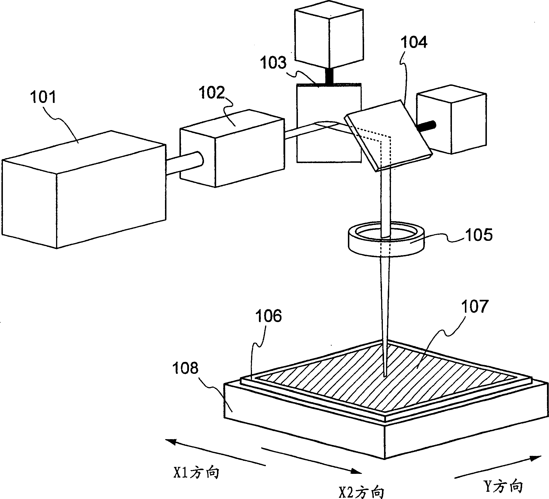
[0157] This example will refer to figure 1 Examples of the present invention will be described.

[0158] 101 denotes a laser oscillator for pulse oscillation, which is a laser oscillator capable of oscillating laser light with a pulse width of picosecond level or less. Any laser can be used for the laser oscillator of the present invention as long as it can oscillate an extremely short-pulse laser beam of 10 psec or less. For example, excimer lasers, Ar lasers, Kr lasers, CO 2 Laser, YAG laser, Y 2 o 3 Laser, YVO 4 Laser, YLF laser, YAlO 3 Laser, GdVo 4 Lasers, ceramic lasers, glass lasers, ruby ​​lasers, alexandrite lasers, Ti:sapphire lasers, copper vapor lasers, or gold vapor lasers, etc.

[0159] This example uses 2W YVO 4 laser. The laser oscillator incorporates a nonlinear optical element, and emits laser light with a wavelength of 532nm at the second harmonic of the laser light, which has a high absorption rate for the amorphous silicon film. It is desirable t...

Embodiment 2

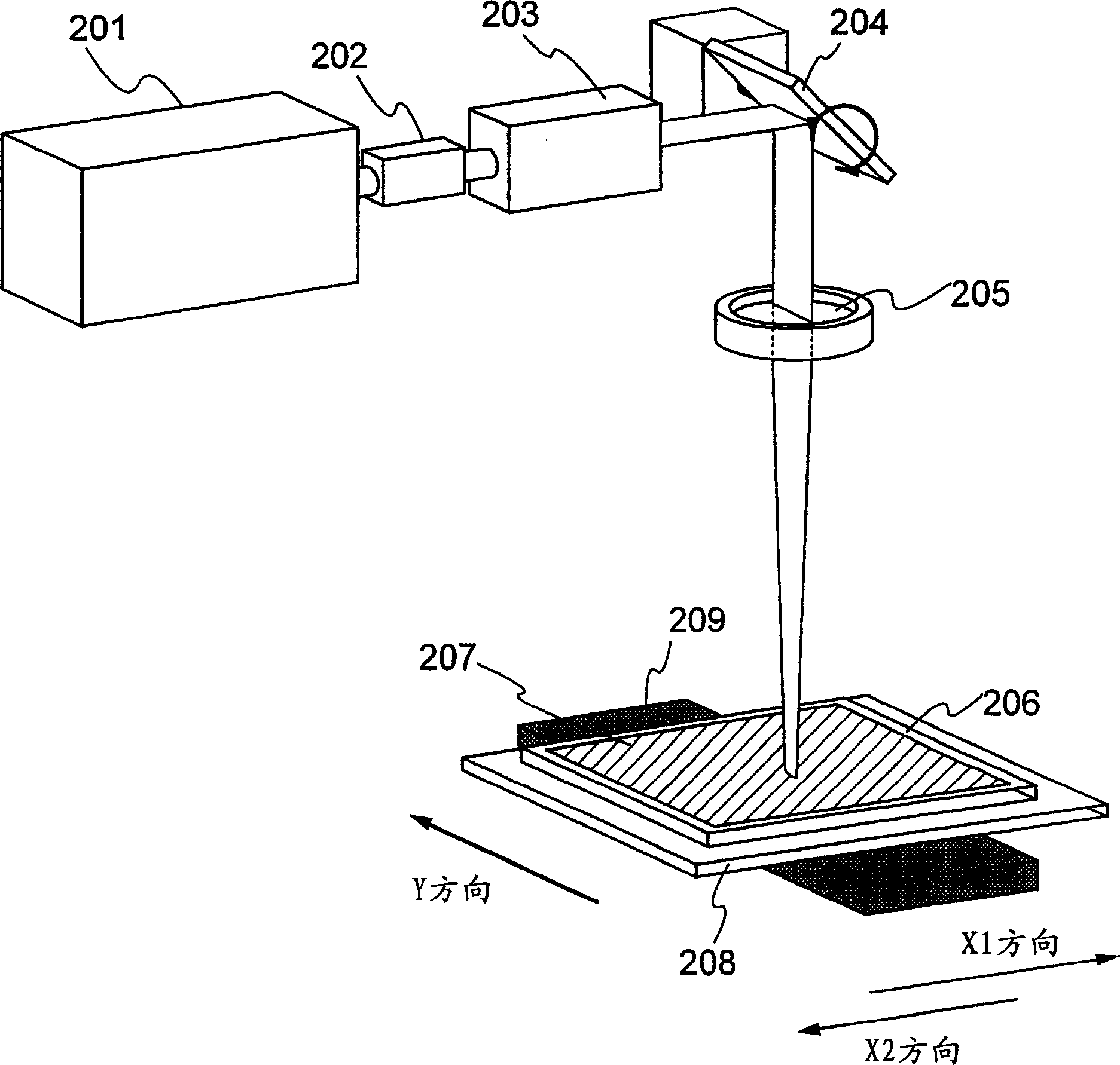
[0174] This example will refer to image 3 An example of a laser irradiation device including a laser oscillator 201 that oscillates laser light with a pulse width of picosecond level or below; an electric mirror 204 driven in one direction; an fθ lens 205 is described. ; The stage 208 and the mobile robot 209 moving in one direction.

[0175] A laser beam output from a laser oscillator 201 is converted into a second harmonic wave by a nonlinear optical element 202 and shaped into an arbitrary shape by an optical system 203 . In this embodiment, the configuration of the optical system 203 is such that the shape of the beam spot on the irradiation surface is formed into a line shape. Thereafter, the semiconductor film 207 formed on the glass substrate 206 is scanned with a linear laser beam (X1 direction) using the galvanic mirror 204 and the fθ lens 205 . Note that, in the case of using a linear beam, laser irradiation can be efficiently performed if the minor axis direction...

Embodiment 3

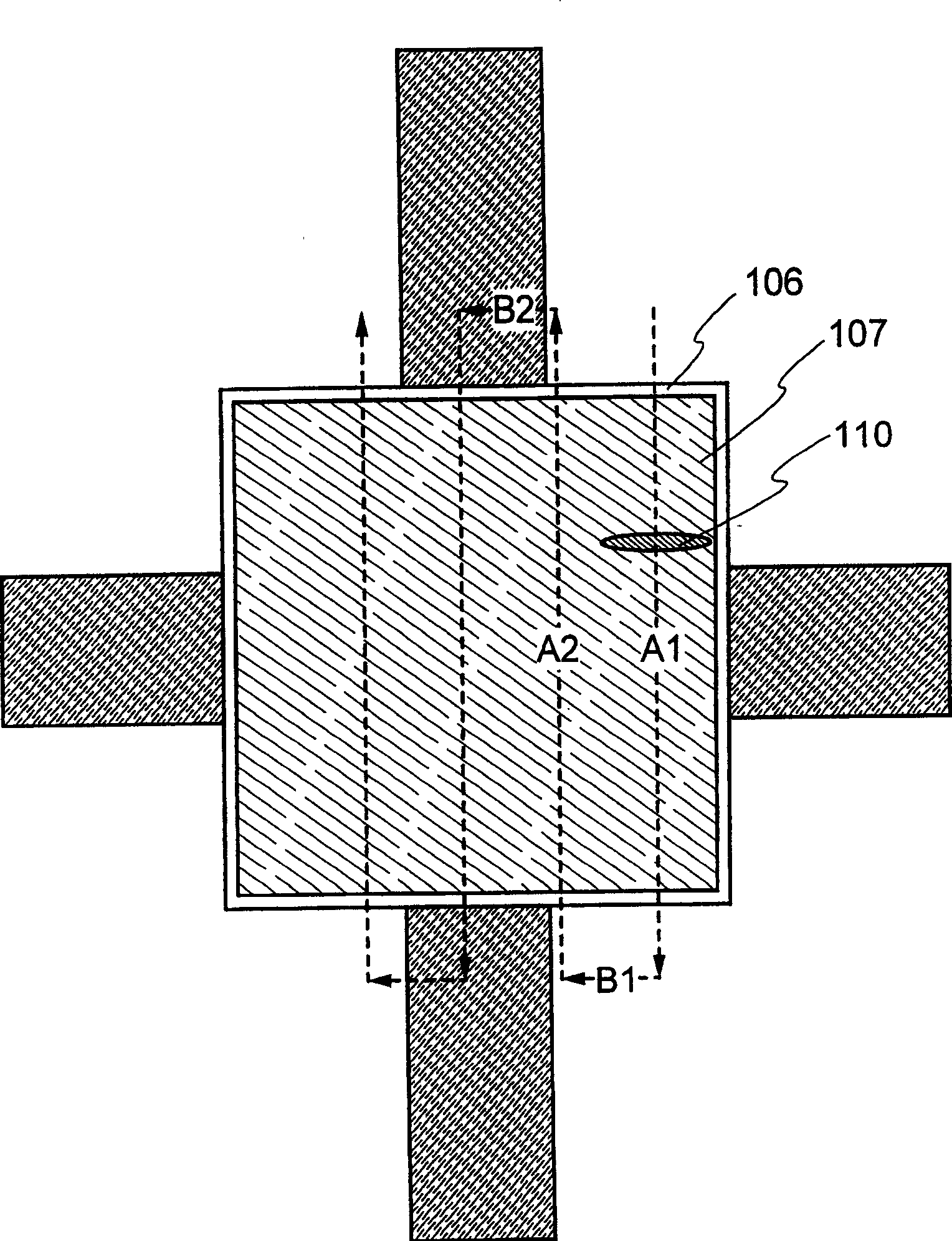
[0180] This example will refer to Figure 4 Another embodiment mode of the present invention will be described. In this embodiment, an example will be described in which laser crystallization is performed only on a position where a TFT is formed in an amorphous semiconductor film formed on a substrate.

[0181] The laser oscillator 401 is a laser oscillator capable of oscillating a laser beam of an extremely short pulse at or below the picosecond level. A laser beam with a pulse width of 10 psec, a wavelength of 532 nm, an output power source of 8 W, a repetition frequency of 80 MHz, and a beam diameter of 0.6 mm was oscillated from this oscillator. The oscillated laser beam is shaped into an arbitrary shape by the optical system 402 . In this embodiment, the beam shape on the semiconductor film 408 formed on the substrate 407 on the irradiation surface is shaped by using a lenticular lens acting only in the uniaxial direction so that the beam shape becomes 300 μm in the maj...


PUM

PropertyMeasurementUnit
Thicknessaaaaaaaaaa
Thicknessaaaaaaaaaa
Thicknessaaaaaaaaaa

Abstract

An object of the present invention is to provide a compact laser irradiation device and a laser irradiation method using an optical system including an electric mirror and an fθ lens, which can suppress interference caused by secondary beams on the back side of a substrate Therefore, uniform laser annealing can be performed on the irradiated object, and the throughput can be improved. In the present invention, when it is assumed that the thickness of the substrate on which the object to be irradiated is formed is d, the refractive index is n, and the speed of light in vacuum is defined as c, the pulse width t of the laser beam satisfies the inequality ct<2nd. In the above structure, even if an optical system including an electric mirror and an fθ lens is used, the influence of interference due to the secondary beams on the backside of the substrate can be reduced, so that uniform laser annealing can be performed on the object to be irradiated.

Description

technical field [0001] The invention relates to a laser irradiation device, a laser irradiation method, and a method for manufacturing a crystalline semiconductor film, in particular to a laser irradiation device and a laser irradiation device using an optical system including an electric mirror (also known as a galvanometer mirror, Galvanometer Mirror) and an fθ lens. An irradiation method and a method for producing a crystalline semiconductor film. Background technique [0002] In laser irradiation equipment, an optical system using a galvanic mirror and an fθ lens is used as one of the methods for scanning the object to be irradiated with a laser beam emitted from a laser oscillator. [0003] By oscillating the galvanic mirror to change the incident angle of the laser beam incident on the galvanic mirror, the position irradiated by the reflected laser beam can be moved, and scanning can be performed in one direction by using a single galvanic mirror. If scanning in the X...

Claims


Application Information

Patent Timeline
IPC IPC(8): H01L21/324H01L21/20H01L21/268H01L21/336H01L29/786H01L51/50H05B33/10
CPCB23K26/0648B23K26/0665B23K26/0853B23K26/064B23K26/082B23K26/0622H01L21/02532H01L21/02686H01L21/02683H01L21/02672H01L21/02422H01L21/324
Inventor 田中幸一郎
Owner SEMICON ENERGY LAB CO LTD
Why Eureka
Try Eureka