Semiconductor integrated circuit device

An integrated circuit and semiconductor technology, applied in the field of semiconductor integrated circuit devices, can solve problems such as restrictions on the formation of public buses, and achieve the effects of increased degrees of freedom, noise prevention, and low impedance

Inactive Publication Date: 2005-07-13
PANASONIC CORP
View PDF0 Cites 7 Cited by
  • Summary
  • Abstract
  • Description
  • Claims
  • Application Information

AI Technical Summary

Problems solved by technology

In order to solve the above problems, when the electrostatic protection circuits are connected together to reduce the number of electrostatic protection circuits, a common bus must be formed. However, the formation of the common bus is limited. When the semiconductor integrated circuit device is miniaturized and highly This is a big problem when integrating

Method used


Image

  • Semiconductor integrated circuit device
  • Semiconductor integrated circuit device
  • Semiconductor integrated circuit device

Examples


no. 1 example

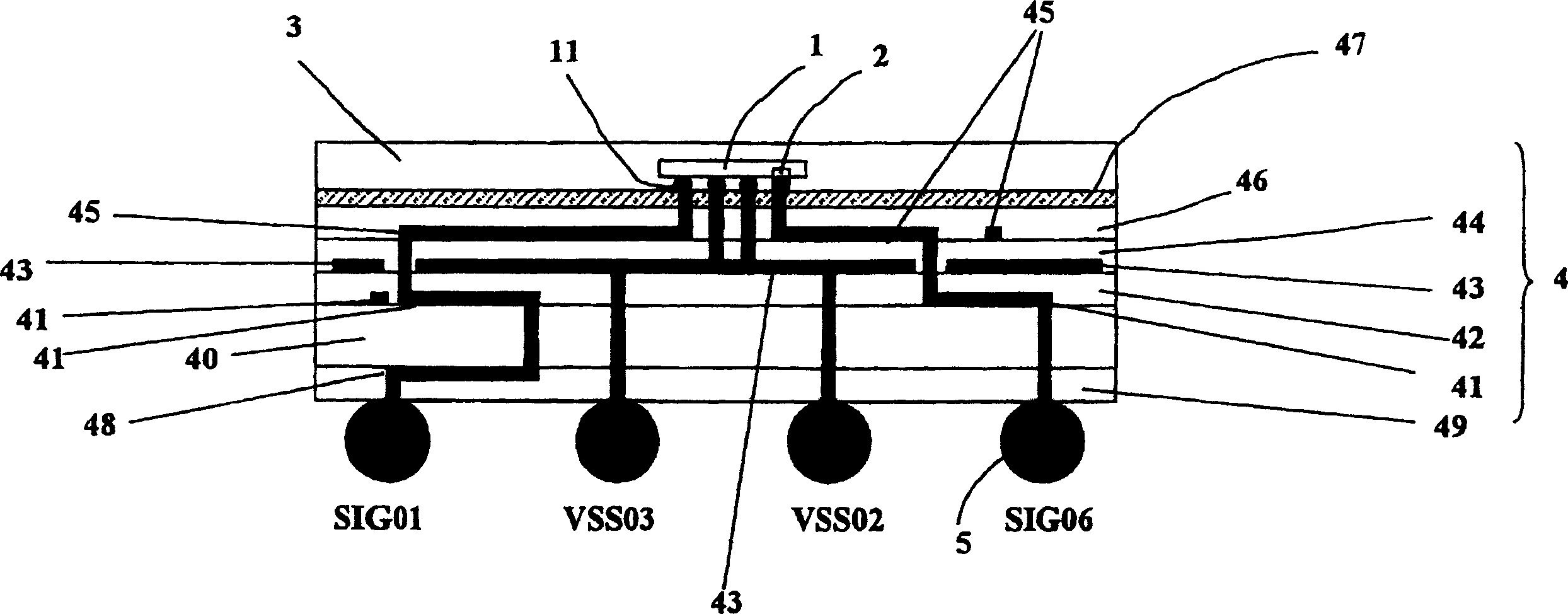
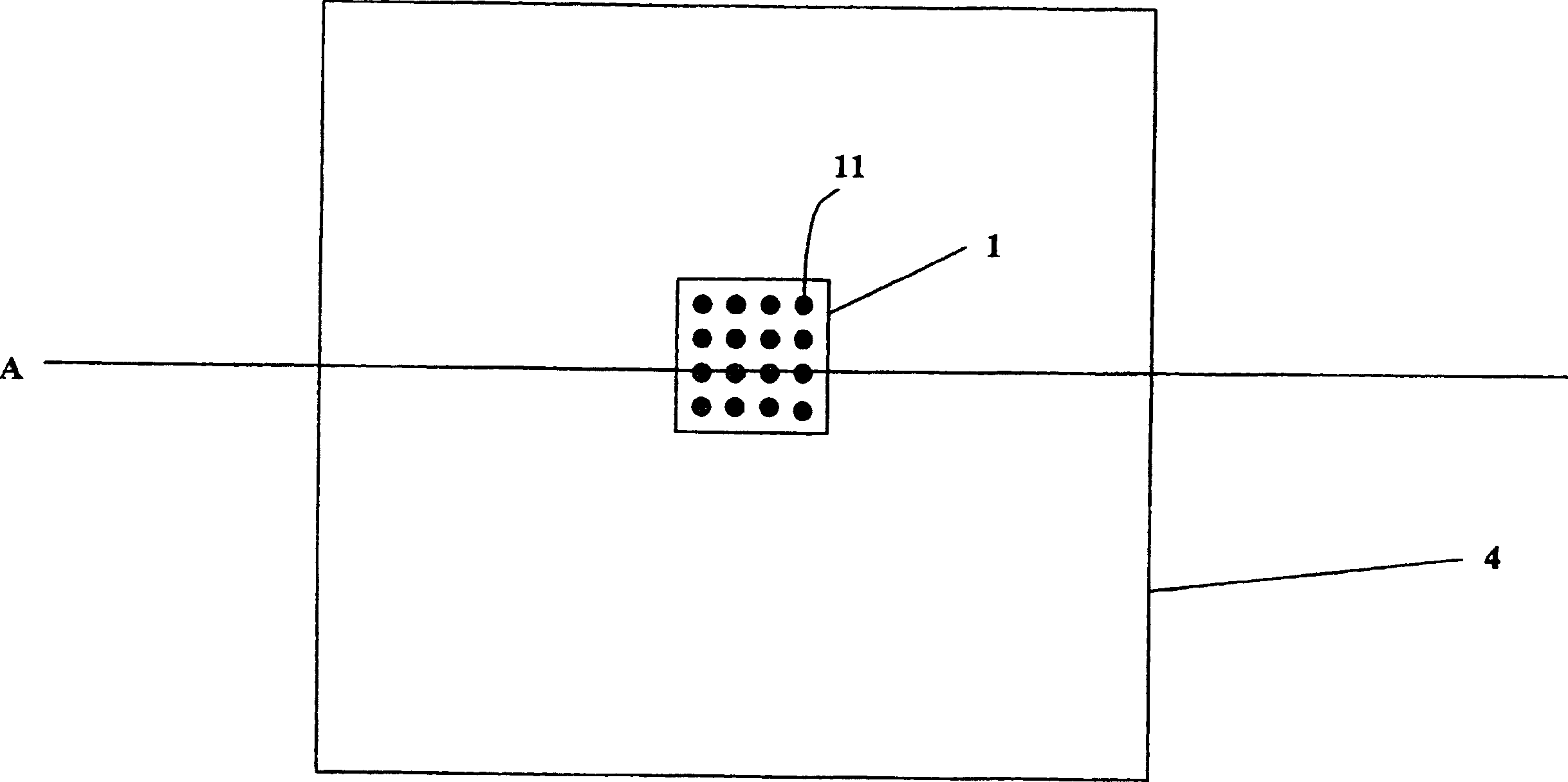
[0068] figure 1 is a cross-sectional view of the structure, Figures 2 to 9 are the plan and cross-sectional views of the semiconductor chip and each layer, such as figure 1 and Figure 2 to Figure 9 As shown, the semiconductor integrated circuit device in this embodiment has the following composition. The semiconductor chip 1 is mounted on a wiring substrate with a multilayer structure having a conductive plane, and is connected to the electrostatic protection circuit 2 provided in the semiconductor chip when the power supply line is connected to the conductive plane 43 . The layers are formed in such a way that when the layers are placed on top of each other, the through-holes overlap each other and the layers are connected to each other via these through-holes.

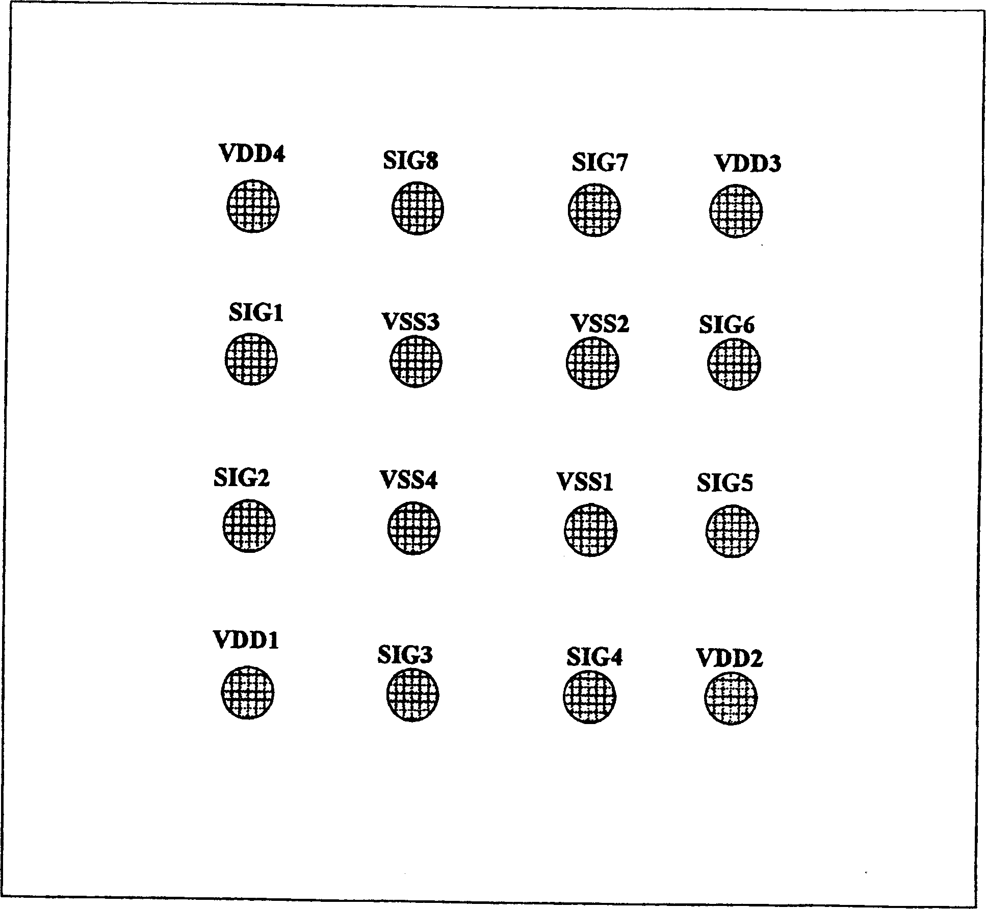
[0069] Such as figure 1 As shown, the device includes: first to fourth circuit systems separately mounted on a semiconductor chip 1 and respectively driven by different power supply systems; ball grid arrays...

no. 2 example

[0086] In this connection, in the above embodiments, the conductive plane 43 formed on the wiring substrate 4 is used as a ground. However, in this example, if Figure 11 , 12(a) and 12(b), in addition to the ground line composed of the conductive plane 43, a conductive plane 43S and an insulating layer 44S are added, and the conductive plane is formed as a power line. On this conductive plane 43S, power supply lines are connected via contacts CD1 to CD4.

[0087] The other points of this structure are the same as those of the first embodiment described above.

[0088] In this connection, the same reference numerals are used for the same components in the first and second embodiments.

[0089] In this structure, not only the ground line is composed of the conductive plane 43 , but also the power line is composed of the conductive plane 43 . Therefore, it is possible to provide a stable potential, and the generation of noise can be attenuated.

no. 3 example

[0091] In this connection, in the previously described embodiments, the conductive plane is connected to one potential. However, in this example, if Figure 13 , 14 As shown in (a) and 14(b), the conductive plane is divided into two parts, the power plane 43b is formed in the outer C-shaped area, and the inner area is used as the ground plane 43a at a predetermined interval. The ground line is connected to this ground plane 43a through contacts C1 to C4. Power lines are connected to this power plane 43b through CD1 to CD4.

[0092] The other points of this structure are the same as those of the first embodiment described above.

[0093] In this connection, the same reference numerals are used for the same parts in the first and third embodiments.

[0094] In this structure, conductive planes with two potentials can be formed on one conductive layer without increasing the number of stacked layers. Therefore, the device can be miniaturized, and the degree of freedom in circ...


PUM


Abstract

A semiconductor integrated circuit device includes: a semiconductor integrated circuit chip installed on a semiconductor substrate, the semiconductor integrated circuit chip is equipped with a plurality of circuit systems, the plurality of circuit systems are separated and driven by different power supply systems, the semiconductor integrated circuit The chip also includes at least one electrostatic protection circuit; and an external connection terminal (5), which is connected to the circuit system of the semiconductor integrated circuit chip through a wiring member (4) having at least one wiring layer, wherein, through the electrostatic protection circuit (2) Power supply lines and ground lines of a plurality of circuit systems of the semiconductor integrated circuit chip (1) are respectively commonly connected to conductive planes (43) provided in the wiring member.

Description

technical field [0001] The invention relates to a semiconductor integrated circuit device, in particular to an insertion structure for inserting an electrostatic protection circuit. Background technique [0002] Generally, in the case of LSI (Large Scale Integration) of a flip-chip system, probe pads are provided on the periphery of a chip, and peripheral circuit elements of the LSI, such as input and output circuit units, are provided at predetermined intervals in an inner region for A power supply unit for an input-output circuit that supplies a power supply voltage to the input-output circuit, and a power supply unit for an LSI internal logic circuit that supplies a power supply voltage to an LSI internal logic circuit. The cell area of ​​the logic circuit inside the LSI is arranged in the inner area of ​​its peripheral circuit elements. [0003] In addition, a rearrangement wiring for connecting pads and LSI is arranged on the surface of the chip. As for power supply l...

Claims


Application Information

Patent Timeline
Patent Type & Authority Applications(China)
IPC IPC(8): H01L23/12H01L21/822H01L23/28H01L23/498H01L23/50H01L23/60H01L27/04
CPCH01L23/49822H01L23/49838H01L23/50H01L23/60H01L2924/01077H01L2924/15173H01L2924/15174H01L2924/15311H01L2924/3011H01L2224/16225H01L2924/10253H01L2224/16235H01L2924/00
Inventor 冈田康幸宫崎浩幸野畑真纯
Owner PANASONIC CORP
Why Eureka
Try Eureka