High-density NROM-FINFET

A memory and storage layer technology, applied in read-only memory, transistor, static memory, etc., can solve problems such as increasing manufacturing cost and reducing integration level

Inactive Publication Date: 2005-10-26
INFINEON TECH AG
View PDF1 Cites 2 Cited by
  • Summary
  • Abstract
  • Description
  • Claims
  • Application Information

AI Technical Summary

Problems solved by technology

Although the required charge pumps are generally known, they require a considerable surface area of ​​the memory chip, thereby reducing its level of integration and increasing its subsequent manufacturing cost.

Method used


Image

  • High-density NROM-FINFET
  • High-density NROM-FINFET
  • High-density NROM-FINFET

Examples


Embodiment Construction

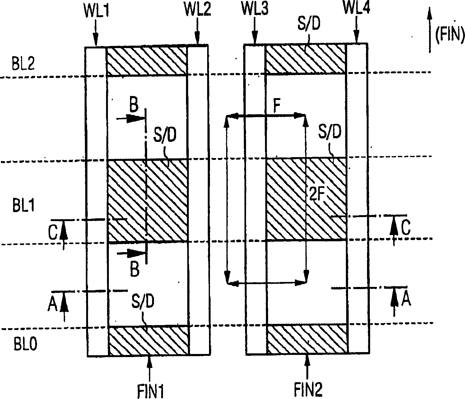
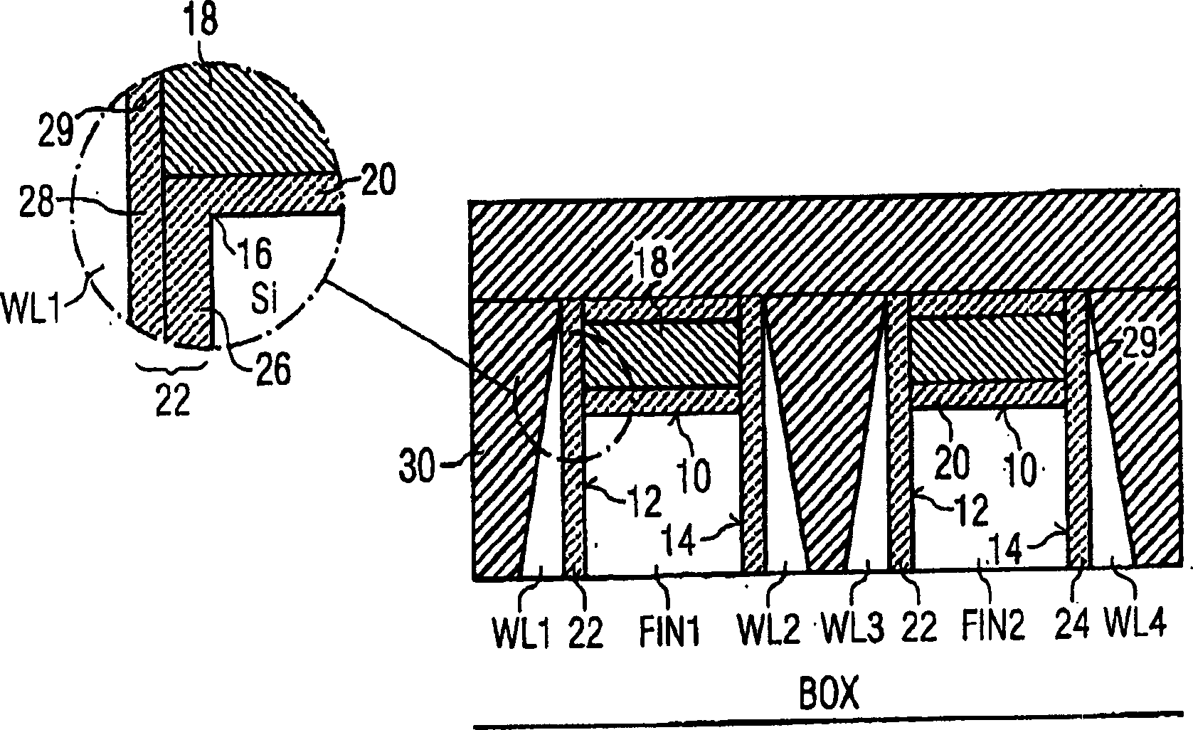
[0056] figure 1 It is a schematic plan view of a memory cell array in a preferred embodiment of a semiconductor memory according to the present invention. The character counties extending along the edges of the two fins made of silicon are labeled WL1, WL2, WL3 and WL4. The first mesh rib extends in the direction indicated by the arrow (FIN) between the word line WL1 and the word line WL2, and is marked as FIN1; the second rib extends between the word line WL3 and the word line WL4 between, and marked as FIN2. Note that, figure 1 Only a small detail of a large array of memory cells is constructed with multiple ribs FIN running parallel to each other and evenly spaced.

[0057] The highly doped contact regions S / D spaced apart from each other by a distance F are located in the ribs FIN and are marked in particular by dotted figures at figure 1 middle. Therefore, the two adjacent contact regions S / D of each rib respectively form the source and drain terminals of a FINFET (F...


PUM


Abstract

Semiconductor memory having memory cells, each including first and second conductively-doped contact regions and a channel region arranged between the latter, formed in a web-like rib made of semiconductor material and arranged one behind the other in this sequence in the longitudinal direction of the rib. The rib has an essentially rectangular shape with an upper side of the rib and rib side faces lying opposite. A memory layer is configured for programming the memory cell, arranged on the upper side of the rib spaced apart by a first insulator layer, and projects in the normal direction of the one rib side face over one of the rib side faces so that the one rib side face and the upper side of the rib form an edge for injecting charge carriers from the channel region into the memory layer. A gate electrode is spaced apart from the one rib side face by a second insulator layer and from the memory layer by a third insulator layer, electrically insulated from the channel region, and configured to control its electrical conductivity.

Description

technical field [0001] The invention relates to a semiconductor memory and a method for manufacturing the semiconductor memory. Background technique [0002] Traditional programmable semiconductor memory components have many different designs depending on the application, such as PROM, EPROM, EEPROM, FLASH EEPROM and SONOS, etc.; the differences between these different designs are especially in erasing options, programming capabilities and programming time, retention time, storage Density, and its manufacturing cost; and at present, high-density and economical flash semiconductor memories are especially required. In particular, conventional designs are about NAND and ETOX memory cells, however their storage density needs to be higher than 4F 2 (Where F is the minimum structural size of the semiconductor memory in the manufacturing process). In the document "NROM: A novellocalized trapping, 2-bit nonvolatile Memory Cell" disclosed by B. Eitan et al. in IEEE Electron Device ...

Claims


Application Information

Patent Timeline
IPC IPC(8): G11C16/04H01L21/28H01L21/336H01L21/8246H01L21/8247H01L21/84H01L27/115H01L27/12H01L29/786H01L29/788H01L29/792H01R11/22H01R13/62
CPCY10S257/905H01L29/785H01L29/7881Y10S257/903H01L29/66825H01L21/845H01L27/11521H01L29/66833H01L27/11568Y10S257/904H01L21/28282H01L29/792G11C16/0466H01L29/66795H01L27/115H01L21/28273H01L27/1203H01L29/40114H01L29/40117H10B43/30H10B69/00H10B41/30H10B41/35
Inventor F·霍夫曼恩E·兰德格拉夫R·J·鲁肯W·雷斯纳M·斯佩奇特
Owner INFINEON TECH AG
Why Eureka
Try Eureka