Imaging interference photo etching method and system by rotating a mask and a resist silicon slice

A technology of imaging interference and resist, which is applied in the direction of microlithography exposure equipment, photolithography exposure device, electrical components, etc., can solve the problems affecting the quality and fidelity of graphics, the difficulty of optical path and graphics alignment, and the reduction of exposure efficiency and other problems, to achieve the effect of improving laser utilization, shortening exposure time, and improving exposure efficiency

Inactive Publication Date: 2005-11-02
INST OF OPTICS & ELECTRONICS - CHINESE ACAD OF SCI
View PDF0 Cites 6 Cited by
  • Summary
  • Abstract
  • Description
  • Claims
  • Application Information

AI Technical Summary

Problems solved by technology

[0005] However, this imaging interference lithography method is difficult to adjust the optical path and pattern alignment in real time betw

Method used


Image

  • Imaging interference photo etching method and system by rotating a mask and a resist silicon slice
  • Imaging interference photo etching method and system by rotating a mask and a resist silicon slice
  • Imaging interference photo etching method and system by rotating a mask and a resist silicon slice

Examples


Embodiment Construction

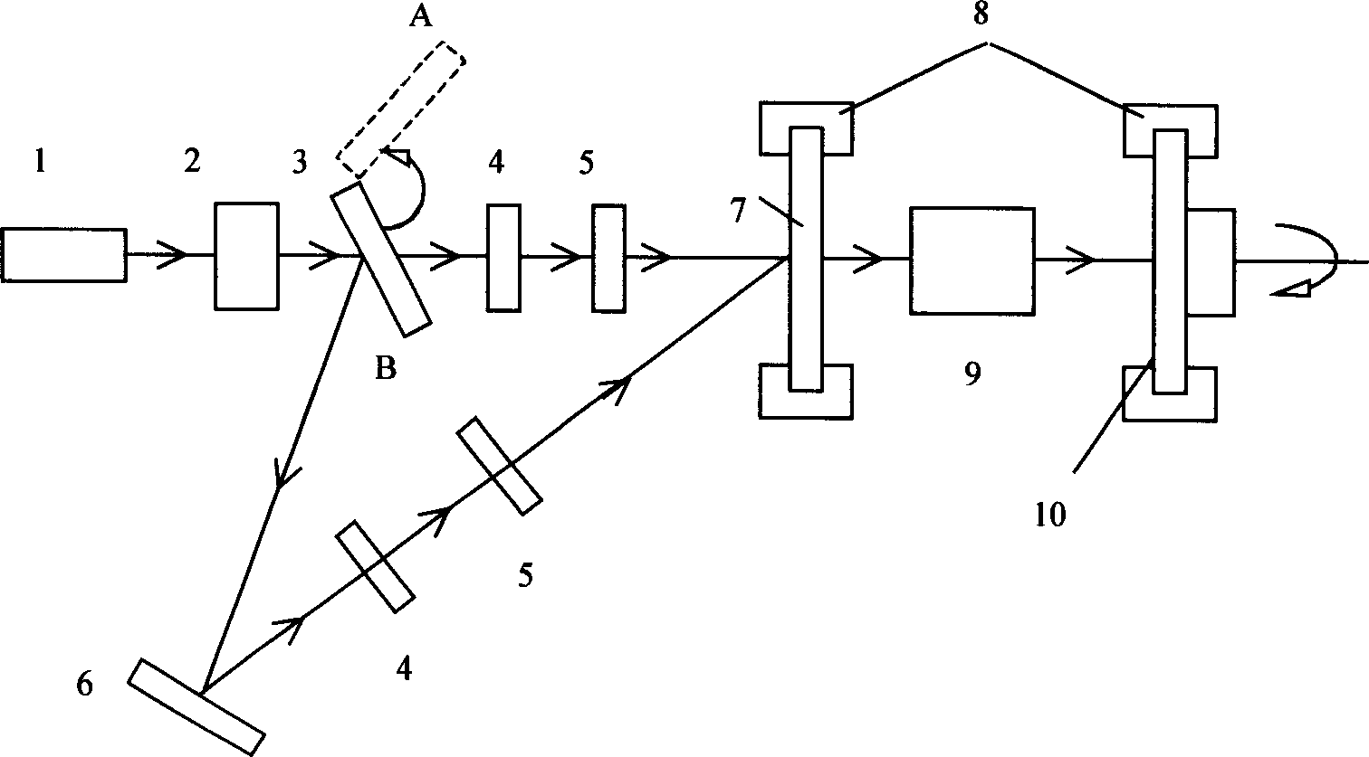
[0019] Such as figure 1 As shown, the embodiment system of the imaging interference lithography method of rotating mask and resist silicon wafer of the present invention includes a laser 1, a beam expander collimator 2, a rotatable total reflection mirror 3, a timing shutter 4, a variable density Neutral filter 5, total reflection mirror 6, mask 7, synchronous rotating mechanism 8, imaging optical system 9 and resist silicon wafer 10. When the rotatable total reflection mirror 3 is placed at the A position, the laser beam emitted by the laser 1 is expanded into a parallel beam through the beam expander collimator 2, and the parallel beam passes through the timing shutter 4 and the variable density neutral filter 5 perpendicularly The mask 7 is illuminated, and the imaging optical system 9 images the mask 7 on the resist silicon wafer 10 to expose the resist for the first time. Afterwards, the rotatable total reflection mirror 3 is transferred to the B position. At this time, ...


PUM


Abstract

Imaging interference photo-etching method of movable mask and resister silicon concerns that, use a precise rotation machine; take low frequency and x direction high frequency component double exposure separated on vertical light illumination mask and x direction oblique illumination mask; rotate the mask and resister with 90Deg synchronously; take y direction high frequency component exposure to realize the third exposure needed by this method, and form high resolution mask image finally. The method is simple, need not use multiple lasers with different wavelength or frequency excursion device; decreases cost, simplifies structure, adjustment and focusing of system; use shutter to control exposure time, variable filter to adjust exposure light intensity rate, holophote of rotating in and out between low and high frequency component exposure to increase laser energy utilance, achieves imaging of high resolution and high quality finally. This invention needs not to adjust light path real-time among exposures, use a laser with one wavelength to realize imaging interference photo-etching, decreases adjustment, focusing difference, and exposure time, and improves exposure efficiency.

Description

technical field [0001] The invention relates to an imaging interference photolithography method and a photolithography system for rotating a mask and resist silicon wafer, and belongs to the improvement and implementation of the imaging interference photolithography method and system for producing high-resolution fine patterns. technical background [0002] Laser interference lithography technology uses the interference between beams to produce periodic pattern arrays. Its limitation is that it can only produce periodic patterns, and it is difficult to produce a variety of arbitrary patterns required for the production of integrated circuits in the microelectronics industry. For this reason, people have proposed an imaging interference lithography technology that can not only improve the resolution but also produce arbitrary patterns. The general imaging interference lithography method uses a mask and a resist silicon wafer to fix, and changes the direction of the illuminati...

Claims


Application Information

Patent Timeline
IPC IPC(8): G03F7/20
Inventor 张锦冯伯儒刘娟宗德蓉
Owner INST OF OPTICS & ELECTRONICS - CHINESE ACAD OF SCI
Why Eureka
Try Eureka