A substrate edge protection device, lithography equipment and protection method

An edge protection and lithography equipment technology, applied in the field of substrate edge protection devices, can solve the problems of reduced reliability of silicon wafers, reduced production efficiency, reduced adsorption reliability, etc., and achieves improved exposure quality and yield, improved production efficiency, and improved adsorption Reliable effect

Active Publication Date: 2021-06-29
SHANGHAI MICRO ELECTRONICS EQUIP (GRP) CO LTD
View PDF5 Cites 0 Cited by
  • Summary
  • Abstract
  • Description
  • Claims
  • Application Information

AI Technical Summary

Problems solved by technology

[0003] With the development of Through Silicon Vias (TSV) technology, the continuous thinning of silicon wafers and the bonding process of silicon wafers lead to uncertain warping of the silicon wafer itself. A gap is formed on the surface. When the suction cup turns on the vacuum, there will be a vacuum leak between the suction cup and the silicon wafer, which cannot meet the vacuum threshold under normal conditions, resulting in a decrease in the reliability of the silicon wafer adsorption, and even the occurrence of the chip, which greatly affects productivity
In addition, the reduced reliability of silicon wafer adsorption will affect the focal depth (focus) and overlay accuracy (overlay) of lithography equipment, which is reflected in the surface accuracy of its upper and lower surfaces and its own clamping deformation, thus affecting the exposure quality of silicon wafers and wafer yield
[0004] The existing technology cannot expose silicon wafers with large warpage. In addition, it is necessary to set up additional protection devices for the edge of the silicon wafer, and transmit the protection ring to complete the upper ring covering the edge of the silicon wafer, so as to protect the edge of the silicon wafer from exposure during the exposure process. It was exposed, in which the protective ring is a kind of light-shielding shielding object with a central part hollowed out and solid edges
This undoubtedly increases the flow and time of the entire exposure process and reduces production efficiency

Method used


Image

  • A substrate edge protection device, lithography equipment and protection method
  • A substrate edge protection device, lithography equipment and protection method
  • A substrate edge protection device, lithography equipment and protection method

Examples


Embodiment 1

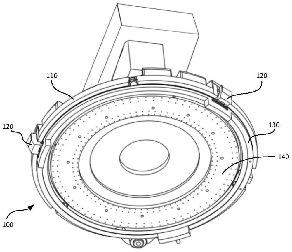
[0050] Embodiment 1 of the present invention provides a substrate edge protection device, figure 1 is a perspective view of the base edge protection device provided by Embodiment 1 of the present invention, figure 2 It is a structural schematic diagram of the warpage processing mechanism in the substrate edge protection device provided in Embodiment 1 of the present invention. Such as figure 1 As shown, the base edge protection device 100 includes a base 110, a grasping part 120 arranged on the working side edge of the base 110, and the grasping part 120 is used to grasp and place the base edge protection ring 130;

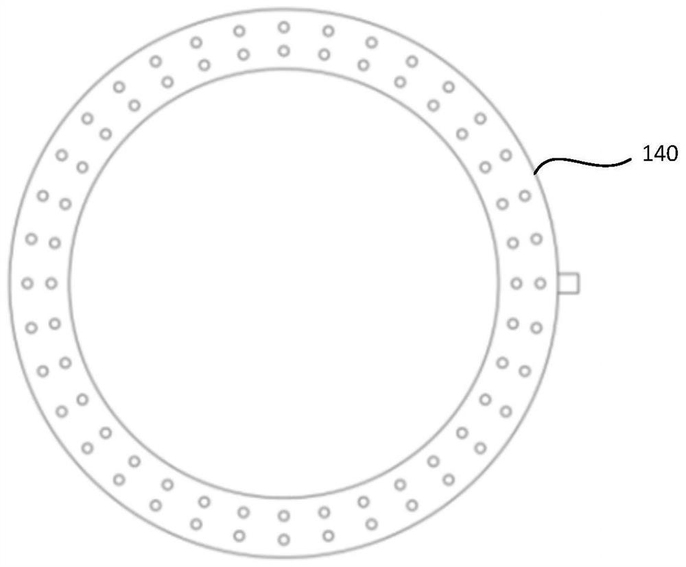
[0051] The warpage processing mechanism 140 arranged on the working side of the base 110, such as figure 2 As shown, the warpage processing mechanism 140 includes a plurality of air blowing holes formed on the working surface, and an air inlet communicating with the air blowing holes, and the warpage processing mechanism 140 is used to blow air through the air...

Embodiment 2

[0061] Embodiment 2 of the present invention provides a lithography equipment, which includes the substrate edge protection device 100 described in Embodiment 1, such as figure 1 As shown, the base edge protection device 100 includes a base 110, a grasping part 120 arranged on the edge of the working side of the base 110, the grasping part 120 is used to grasp and fix the base edge protection ring 130; Warp processing mechanism 140, warp processing mechanism 140 includes a plurality of blowing holes formed on the working surface, and an air inlet connected with the blowing holes, warping processing mechanism 140 is used to blow air through the blowing holes to level the substrate .

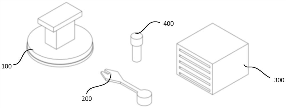
[0062] The lithography equipment also includes a workpiece table, the substrate edge protection device 100 is located directly above the workpiece table of the lithography equipment, and can move in the vertical direction; the working side of the substrate edge protection device 100 is facing the ...

Embodiment 3

[0072] Embodiment 3 of the present invention provides a protection method for a substrate edge protection device, Figure 5 It is a flow chart of a protection method of a substrate edge protection device provided in Embodiment 3 of the present invention. refer to figure 1 , the base edge protection device 100 includes a base 110, a grasping part 120 arranged on the edge of the working side of the base 110, the grasping part 120 is used to grasp and fix the base edge protection ring 130; Mechanism 140, the warpage processing mechanism 140 includes a plurality of blowing holes formed on the working surface, and an air inlet connected to the blowing holes, and the warpage processing mechanism is used to blow air through the blowing holes to level the substrate. The substrate edge protection device 100 is located in a lithography equipment, and the lithography equipment also includes a manipulator 200 and a workpiece table. Such as Figure 5 As shown, the method includes:

[0...


PUM


Abstract

The invention discloses a substrate edge protection device, photolithographic equipment and a protection method. Wherein, the base edge protection device includes a base, a grasping part arranged on the edge of the working side of the base, used for grabbing and fixing the base edge protection ring, and a warping processing mechanism on the working side of the base, and the working surface of the warping processing mechanism has A plurality of air blowing holes, and an air inlet connected with the air blowing holes, blow air through the air blowing holes to level the substrate. In the substrate edge protection device provided by the embodiment of the present invention, a warpage treatment mechanism is provided on the working side of the base, and positive pressure gas is blown to the warped substrate on the workpiece table through the warpage treatment mechanism to level the warped substrate and completely absorb the substrate. On the suction cup, the leveling of the substrate with a large amount of warpage is realized, which improves the substrate exposure quality and yield; in addition, the substrate shaping and the placement of the substrate edge protection ring can be realized through the substrate edge protection device, which simplifies the exposure process. Thereby improving production efficiency.

Description

technical field [0001] Embodiments of the present invention relate to the field of semiconductor manufacturing, and in particular to a substrate edge protection device, photolithography equipment and protection method. Background technique [0002] Lithography equipment is mainly used in the manufacture of integrated circuits IC or other micro devices. With photolithographic equipment, a mask pattern is imaged onto a photoresist-coated substrate, usually a silicon wafer. The substrate is usually fixed by the sucker on the workpiece table through vacuum adsorption, and the workpiece table drives the sucker with the silicon wafer to move, and reaches the correct position according to the predetermined route and speed to complete the photolithography process. [0003] With the development of Through Silicon Vias (TSV) technology, the continuous thinning of silicon wafers and the bonding process of silicon wafers lead to uncertain warping of the silicon wafer itself. A gap is ...

Claims


Application Information

Patent Timeline
Patent Type & Authority Patents(China)
IPC IPC(8): G03F7/20
CPCG03F7/70733G03F7/70783G03F7/20
Inventor 曹文郎东春
Owner SHANGHAI MICRO ELECTRONICS EQUIP (GRP) CO LTD
Why Eureka
Try Eureka