
Multilayer chip ZnO varistor prepared by nano material and manufacturing method

A varistor and nanomaterial technology, applied in varistor core, resistor manufacturing, varistor and other directions, can solve the problem of reducing the nonlinear coefficient of varistor, increasing the leakage current of varistor, Resistance performance deterioration and other problems, to achieve the effect of saving production steps, reducing usage, and improving efficiency

Inactive Publication Date: 2005-11-09
HENAN JINGUAN WANGMA INFORMATION INDAL
View PDF3 Cites 17 Cited by
  • Summary
  • Abstract
  • Description
  • Claims
  • Application Information

AI Technical Summary

Problems solved by technology

Chinese patent CN1564270A "low-temperature sintering ZnO multilayer chip varistor and its manufacturing method" discloses a low-temperature sintering additive (mainly composed of Bi 2 o 3 , Sb 2 o 3 , B 2 o 3 、TiO 2 composition) to reduce the sintering temperature of varistor ceramics, but B 2 o 3 Reacts with water, making material handling difficult in the ball milling process, TiO 2 It will reduce the nonlinear coefficient of the varistor and increase the leakage current of the varistor, making the performance of the varistor worse

Method used


Image

  • Multilayer chip ZnO varistor prepared by nano material and manufacturing method
  • Multilayer chip ZnO varistor prepared by nano material and manufacturing method

Examples


Embodiment 1

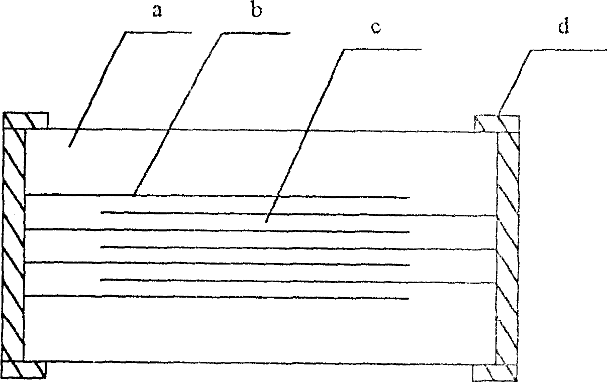
[0038] Such as figure 1 structure shown, figure 2 The manufacturing method process shown, and according to formula table 1, accurately weigh the oxides of the nano-ZnO powder that the average particle diameter is 99nm and the various nano-powder additives that the average particle diameter is 99nm, put the weighed material into Add appropriate amount of xylene, binder, dispersant and zirconium balls to the ball mill, mill for 12 hours to obtain casting slurry, and then cast a ceramic film tape with a thickness of 25 microns, and press the ten-layer ceramic film tape slightly A film with a thickness of about 250 microns is obtained, and an alloy internal electrode b with a weight ratio of 75% silver and 25% palladium is printed on the film with a protective layer a, and another layer of internal electrodes is printed in a misplaced manner after lamination until The effective layer c is 8 layers. After isostatic pressure, the sintered green body with a size of 1.0×0.5mm is cut...

Embodiment 2

[0041] Such as figure 1 structure shown, figure 2 The manufacturing method process shown, and according to the formula table two, accurately weigh the oxides of the nano-ZnO powder with an average particle diameter of 1nm and various nano-powder additives with an average particle diameter of 1nm, and put the weighed materials into Add appropriate amount of xylene, binder, dispersant and zirconium balls to the ball mill, mill for 12 hours to obtain casting slurry, and then cast a ceramic film tape with a thickness of 25 microns, and press the ten-layer ceramic film tape slightly A film with a thickness of about 250 microns is obtained. On the film with a protective layer a, an alloy internal electrode b with a weight ratio of 89% silver and 11% palladium is printed, and another layer of internal electrodes is printed in a misplaced manner after lamination until The effective layer c is 8 layers. After isostatic pressure, the sintered green body with a size of 1.0×0.5mm is cut...

Embodiment 3

[0044] Such as figure 1 structure shown, figure 2 According to the manufacturing method flow shown, accurately weigh the composite nano-particles containing Zn and Bi, Sb, Mn, Si, Cr, Co, Ni, Al and other elements with an average particle size of 40nm according to the formula table three. Oxide powder, put the weighed material into a ball mill and add an appropriate amount of xylene, binder, dispersant and zirconium balls, ball mill for 12 hours to obtain a cast slurry, and then cast a 25 micron thick Ceramic membrane strips, ten layers of ceramic membrane strips are slightly pressed to obtain a membrane strip protective layer a with a thickness of about 250 microns, and an alloy internal electrode b with a weight ratio of 85% silver and 15% palladium is printed on the film strip protective layer a, and the laminated After one layer, another layer of internal electrodes is printed in dislocation until the effective layer c is 8 layers. After isostatic pressure, the sintered ...


PUM

PropertyMeasurementUnit
The average particle sizeaaaaaaaaaa

Abstract

The invention discloses a multi-layer chip style of ZnO pressure sensitive resistor made from nanometer materials. It is jointly sintered by the ZnO porcelain material made from nanometer materials and inner electrode layer crossways arranged. Its main characteristic are as follows. The granule shape of the main material of the ZnO porcelain material is orbicular or approximately orbicular. The ZnO nanometer power body of 1 - 99 nm average granule radius, add 3 - 8 % (mol percent) nanometer power body additive whose granule shape is orbicular or approximately orbicular. The said inner electrode layer is Pd / Ag inner electrode layer, in which the Pd proportion is 11 - 25 % of the weight of Pd / Ag inner electrode, and the Ag proportion is 75 - 89 % of the weight of Pd / Ag inner electrode. The ZnO porcelain material and the Pd / Ag inner electrode layer are crossways arranged, and are made by sintering in the temperature bound of 950 - 1100 Deg. C. The present invention also discloses a kind of manufacturing method of the said multi-layer piece style of ZnO pressure sensitive resistor made from nanometer materials. The non-linear coefficient alphaof the multi-layer piece style of ZnO pressure sensitive resistor of 1005 specification made by the present invention is over 20, leaking current IL is less than 2.0 mA.

Description

technical field [0001] The invention relates to a multilayer chip varistor, in particular to a multilayer chip ZnO varistor made of nanomaterials; the invention also relates to a multilayer chip ZnO varistor made of such nanomaterials. How resistors are made. Background technique [0002] In the existing technology, varistors can be divided into high-temperature firing and low-temperature firing according to the sintering temperature: high-temperature firing is 1150°C to 1250°C; low-temperature firing is a low-temperature section around 900°C. The firing temperature of traditional multilayer chip ZnO varistor ceramics exceeds 1150°C, so expensive electrode pastes with high content of precious metals such as silver palladium and silver platinum must be used, and the cost is high. The inner electrode used for high-temperature sintering is 70% silver / 30% palladium inner electrode, even if pure palladium or pure platinum inner electrode is used, the content of precious metal rh...

Claims


Application Information

Patent Timeline
IPC IPC(8): H01C7/112H01C17/30
CPCH01C17/30H01C7/112C04B35/453B32B18/00C04B2237/34C04B2237/68C04B2235/3284C04B2235/781C04B2235/528C04B2235/3294C04B2235/3298C04B2235/3263C04B2235/3241C04B2235/3418C04B2235/3275C04B2235/3279C04B2235/3217C04B2235/443
Inventor 吕呈祥王兰义景志刚杜辉张金秀王雅林魏书周郑慎飞
Owner HENAN JINGUAN WANGMA INFORMATION INDAL
Learn More