Development of photolithographic masks for semiconductors

A technology of photoresist layer and development method, which is applied in the directions of optics, photography, and optomechanical equipment, can solve the problems of photoresist dumping, insufficient hardness, and increased capillary force of photoresist, etc. To achieve the effect of reducing dumping

Active Publication Date: 2005-11-16
TAIWAN SEMICON MFG CO LTD
View PDF2 Cites 8 Cited by
  • Summary
  • Abstract
  • Description
  • Claims
  • Application Information

AI Technical Summary

Problems solved by technology

[0007] However, if other drying processes are performed before the final drying step, additional photoresist dumping is likely to occur, severely reducing yield and process window.
However, when a short-wavelength light source is used to irradiate the photoresist, the phenomenon of photoresist dumping will be more serious. For example, the photoresist after being irradiated with a 193 nm light source will not be as hard as that of a longer wavelength such as Result after irradiation with 248nm light source
Additionally, the capillary forces that cause photoresist topple over increase as the pattern size shrinks

Method used


Image

  • Development of photolithographic masks for semiconductors
  • Development of photolithographic masks for semiconductors
  • Development of photolithographic masks for semiconductors

Examples


Embodiment 1

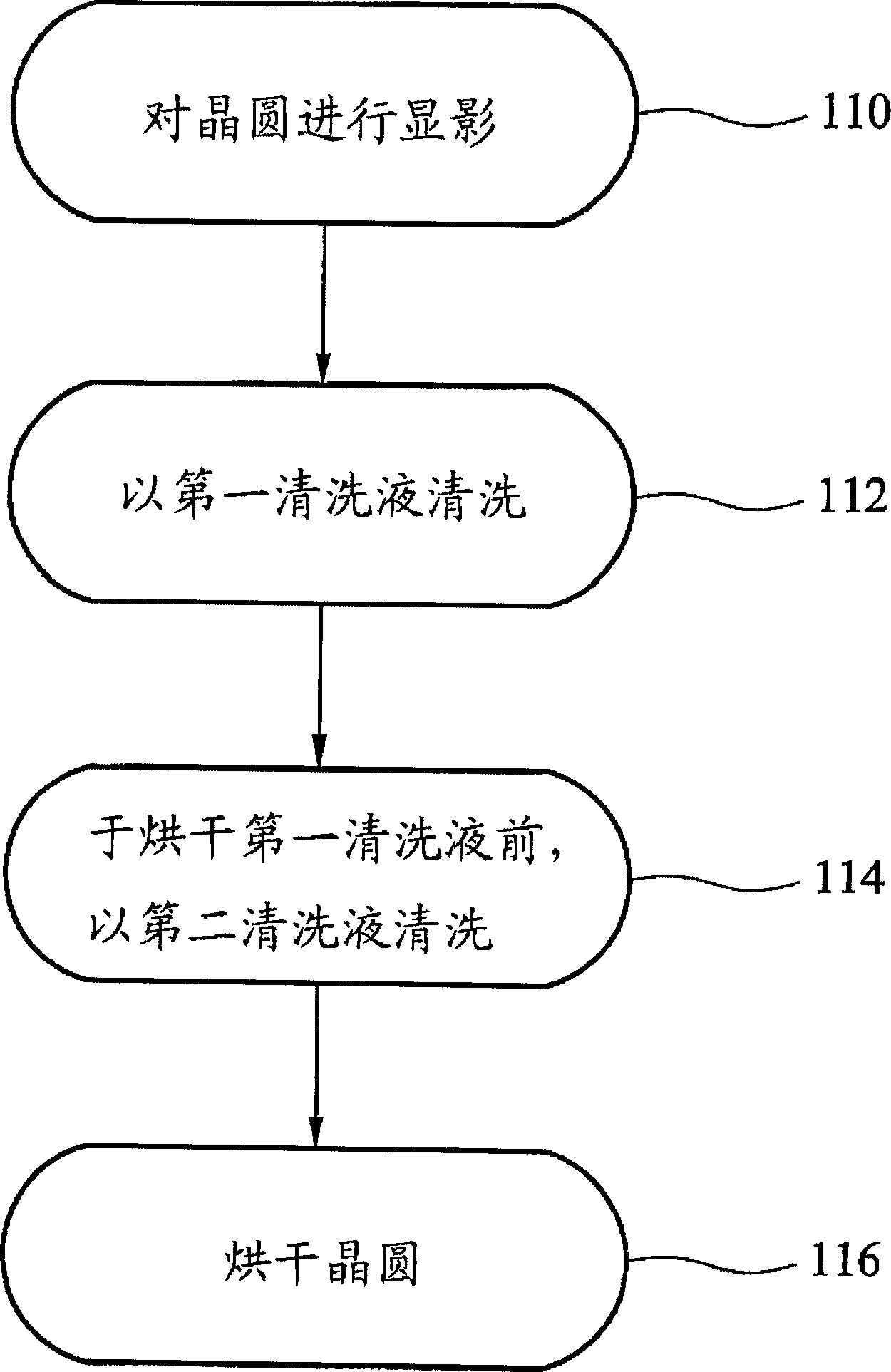
[0036] The process steps disclosed here start from photoresist development, and assume that the photoresist layer on the wafer has been patterned and exposed. The process steps disclosed in the present invention can be combined with an exposure light source with a wavelength lower than or equal to 193 nanometers, and are quite suitable for application in immersion lithography with an exposure wavelength lower than or equal to 248 nanometers.

[0037] figure 1 It is a flow chart of making a photoresist mask according to an embodiment of the present invention. The fabrication flow begins with a developing step at step 110 . The developing step includes any known method of supplying a developer, for example, standing, soaking, spraying, stirring, and the like. In this embodiment, an alkaline solvent with a pH value greater than 9 is provided as a developing solution, for example, tetramethyl ammonium hydroxide (TMAH), and its concentration is generally between 0.1% and 2.8%.

...

Embodiment 2

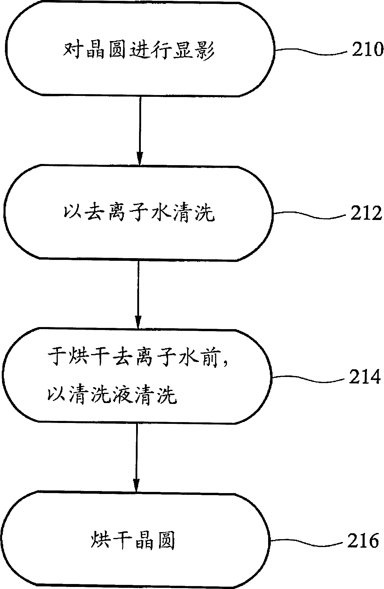
[0045] figure 2 It is a flow chart of making a photoresist mask according to another embodiment of the present invention. The fabrication process begins with a developing step at step 210 . This development step is associated with figure 1 Step 110 is substantially similar.

[0046] Next, perform steps 212 and 214, provide deionized water and cleaning solution to clean the wafer respectively, first clean the wafer with water or deionized water, and then clean it with cleaning solution, and these cleaning steps are all performed before the wafer is dried Finish. As mentioned above, if the wafer is dried before the cleaning step, the photoresist pattern may be dumped. Therefore, between steps 212 and 214, it must be confirmed that there is no wafer drying procedure.

[0047] Cleaning fluids include salt solutions, ionic surfactants, nonionic surfactants, acid solutions, or solutions of dissolved gases. Dissolved gas solutions optionally include dissolved carbon dioxide (C...

Embodiment 3

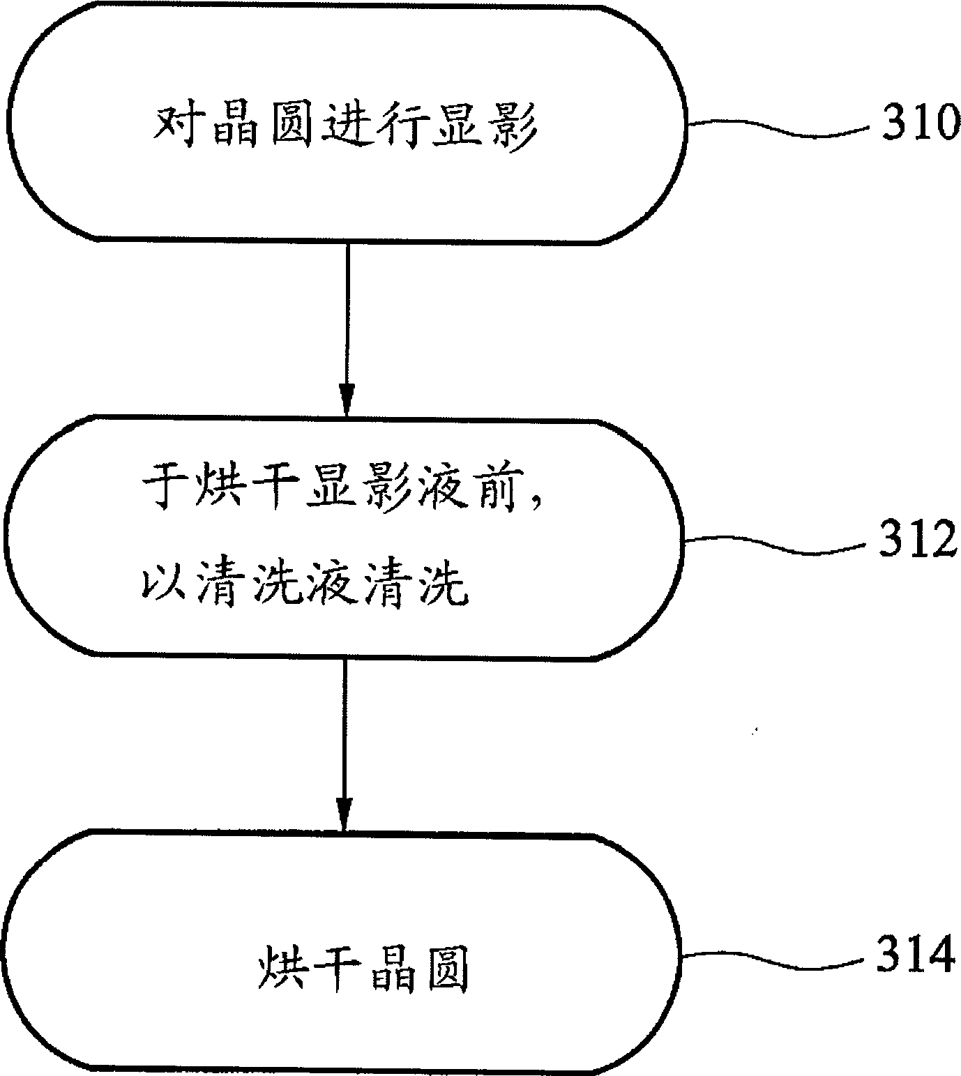
[0051] image 3 It is a flow chart of making a photoresist mask according to another embodiment of the present invention. The fabrication process begins with a development step at step 310 . This development step is associated with figure 1 Step 110 is substantially similar.

[0052] Next, proceed to step 312 , provide a cleaning solution to clean the wafer, and then use the cleaning solution to clean the wafer after the developing step is completed, and the cleaning step must be completed before the wafer is dried. As mentioned above, if the wafer is dried before the cleaning step, the photoresist pattern may be dumped. Therefore, it is necessary to confirm that there is no wafer drying procedure between the developing step and the cleaning step.

[0053] Cleaning fluids include salt solutions, ionic surfactants, nonionic surfactants, acid solutions, or solutions of dissolved gases. Dissolved gas solutions optionally include dissolved carbon dioxide (CO 2 ), sulfur diox...


PUM

PropertyMeasurementUnit
wavelengthaaaaaaaaaa

Abstract

A method of forming a photolithographic mask for use in fabricating a semiconductor device is provided. The method includes forming a layer of photoresist material on a wafer and exposing the photoresist material to a light source. The photoresist material is developed, and before the wafer dries, the wafer is cleaned with one or more cleaning liquids. The cleaning liquid may be a surfactant, an acid, a dissolved gas solution (e.g., CO2, SO2, SO3, NH3, NO2, or the like), deionized water, or the like. Thereafter, the wafer is dried. The wafer may be dried, for example, by a spin dry process, a gas purge process using, for example, compressed dry air, N2, CO2, Ar, or the like, or a drying alcohol such as IPA vapor. The method of the present invention decreases the toppling of the photoresist layer pattern.

Description

technical field [0001] The present invention relates to a semiconductor technology, and more particularly to a method of forming a photoresist mask used in the manufacture of a semiconductor device. Background technique [0002] Generally, the process of manufacturing semiconductor devices includes lithography technology. The lithography step is as follows, firstly, a photoresist material layer is provided, then, the photoresist layer is subjected to pattern exposure, and then, a part of the photoresist layer is removed by development to expose The material layer located under the photoresist layer, after removing excess photoresist, completes the production of a photoresist mask, and then performs an etching step, the above-mentioned layer located under the photoresist layer The material layer is etched to obtain a final pattern due to the protection of the photoresist mask. [0003] Photoresist materials include negative photoresist and positive photoresist. Since the e...

Claims


Application Information

Patent Timeline
Patent Type & Authority Applications(China)
IPC IPC(8): G03F7/20G03F7/30G03F7/32G03F7/40
CPCG03F7/2041G03F7/40
Inventor 张庆裕
Owner TAIWAN SEMICON MFG CO LTD
Why Eureka
Try Eureka