Semiconductor device and display device

A technology for display devices and semiconductors, applied in the field of transistors in circuits, can solve problems such as dispersion of TFT conduction current characteristics, uneven particle size of polycrystalline silicon, etc., and achieve the effect of improving reliability

Inactive Publication Date: 2005-11-23
SANYO ELECTRIC CO LTD
View PDF1 Cites 8 Cited by
  • Summary
  • Abstract
  • Description
  • Claims
  • Application Information

AI Technical Summary

Problems solved by technology

In order to obtain polysilicon, the polycrystallization of amorphous silicon proceeds by laser heat treatment, and the particle size of polysilicon is uneven due to the energy dispersion in the irradiation surface of the irradiated laser
There is a problem that if the dispersion of the particle size is caused (especially if the dispersion is caused near the TFT channel), the on-current characteristics of the TFT will also be dispersed.

Method used


Image

  • Semiconductor device and display device
  • Semiconductor device and display device
  • Semiconductor device and display device

Examples


Embodiment 1

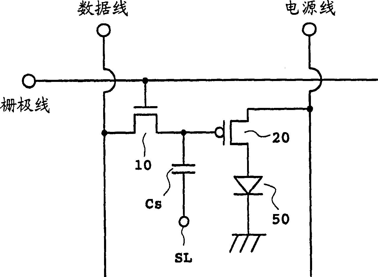
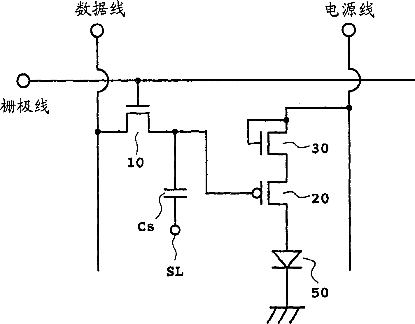
[0060] figure 2 The circuit structure of each pixel in the m-rows-n-columns active matrix type EL display device of Embodiment 1 of the present invention is shown. As shown in the figure, each pixel includes an organic EL element 50, a switching TFT (first TFT) 10, an element driving TFT (second TFT) 20, and a storage capacitor Cs. GL and the area surrounded by the data lines DL extending in the column direction. In this embodiment, a compensating TFT 30 having a conductivity characteristic opposite to that of the second TFT 20 is inserted between the power supply line VL and the second TFT 20 . The gate of the TFT 30 for compensation is connected to one of the source and the drain to form a diode, and the diode is connected in a forward direction between the power supply line VL and the second TFT 20 . Accordingly, it is possible to operate without supplying a special control signal.

[0061] The gate of the first TFT 10 receives a gate signal and is turned on. Thus, the ...

Embodiment 2

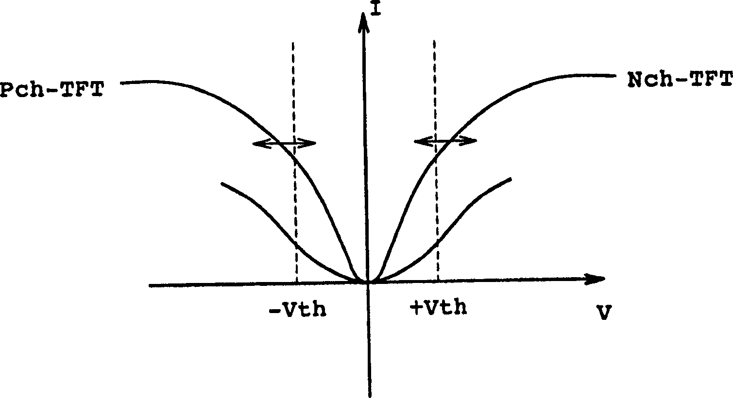
[0110] Next, another embodiment 2 of the present invention will be described. In Example 1, in order to prevent dispersion of light emission luminance between pixels due to dispersion of transistor characteristics, a thin film transistor for compensating which has an opposite conduction characteristic to that of the thin film transistor for driving an element is provided. On the other hand, in the second embodiment, attention is paid to the arrangement of the element-driving thin film transistors (second TFTs) to suppress the dispersion of light emission luminance among pixels. FIG. 10 shows a configuration example of each pixel in Embodiment 2, FIG. 10( a ) is a schematic plan view, and FIG. 10( b ) is a cross-sectional view along line B-B of FIG. 10( a ). The structure starts with figure 1 The same circuit configuration is shown. In addition, in the figure, the same code|symbol is attached|subjected to the part corresponding to the figure already demonstrated.

[0111] In...

Embodiment 3

[0128] Next, as a third embodiment, a more efficient connection method of a plurality of second TFTs 20 and corresponding organic EL elements 50 in one pixel will be described. As above-mentioned embodiment 1 and embodiment 2 Figure 11 As shown in , it is preferable to provide a plurality of second TFTs 20 between the organic EL element 50 and the power supply line VL in one pixel from the viewpoint of improving reliability and improving characteristics. In the case of setting a plurality of 2nd TFTs 20 in one pixel, as Figure 11 As shown, by connecting the second TFTs 20 a and 20 b to the organic EL element 50 , the current supply from the power line VL to the organic EL element 50 through the second TFT 20 is more reliable. However, in the case of an organic EL element of the type that emits light from the light emitting layer 55 to the outside through the substrate 1 below from the transparent anode 52 as shown in FIG. For example, in Figure 9 (c) or in FIG. 10( b), t...


PUM


Abstract

The objective is to reduce variation of a current to be supplied to a plurality of organic EL elements. An element drive TFT 20 for controlling a current value to be supplied from a power supply line VL is provided between an organic EL element 50 and a power supply line VL, and the channel length direction of the TFT 20 is arranged in parallel with the lengthwise direction of a pixel, or with the extending direction of a data line for supplying a data signal to a switching TFT for controlling the TFT 20, or the scanning direction of laser annealing for polycrystallizing the active layer 16 of the TFT 20. Furthermore, a compensating TFT 30 of an inverse TFT 20 having inverse characteristics may be provided between the power supply line VL and the TFT 20.

Description

[0001] This application is a divisional application of the invention patent application with the filing date of September 29, 2001, the application number of 01138517.0, and the invention title of "semiconductor device and display device". field of invention [0002] The present invention relates to an electroluminescent display device, and more particularly to a transistor constituting a circuit of a pixel portion therein. Background technique [0003] An EL display device in which an electroluminescence (hereinafter referred to as EL) element of a self-luminous element is used as a light-emitting element in each pixel is a self-luminous type, and at the same time, it has advantages such as a thin device and low power consumption. A display device that replaces a display device such as a liquid crystal display device (LCD) or a CRT is attracting attention and research is being conducted. [0004] Among them, an active matrix EL display device in which a switching element su...

Claims


Application Information

Patent Timeline
Patent Type & Authority Applications(China)
IPC IPC(8): G09F9/33
Inventor 安斋胜矢古宫直明
Owner SANYO ELECTRIC CO LTD
Why Eureka
Try Eureka