Surface high reflective semiconductor saturable absorption mirror

A saturable absorption, semiconductor technology, used in laser parts, electrical components, lasers, etc.

Inactive Publication Date: 2005-12-14
INST OF SEMICONDUCTORS - CHINESE ACAD OF SCI
View PDF0 Cites 4 Cited by
  • Summary
  • Abstract
  • Description
  • Claims
  • Application Information

AI Technical Summary

Problems solved by technology

When making a high-power mode-locked laser, the traditional semi...

Method used


Image

  • Surface high reflective semiconductor saturable absorption mirror
  • Surface high reflective semiconductor saturable absorption mirror

Examples


Embodiment

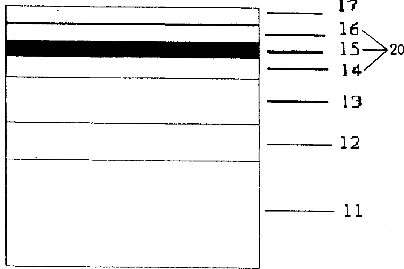
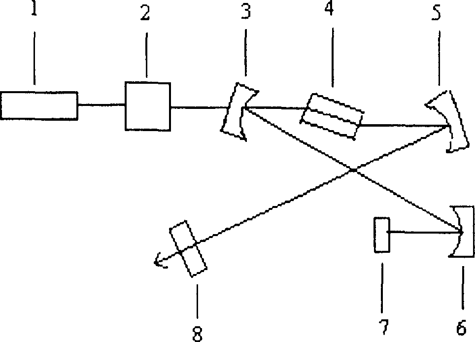
[0028] The surface high inversion semiconductor saturable absorbing mirror of the present invention is suitable for the passive mode-locked cavity structure of the solid-state laser with a wavelength near 1060nm, and is suitable for figure 2 The X-cavity structure shown. see figure 2 , the Yb:YAG passively mode-locked laser of the present embodiment comprises 940nm semiconductor pump source 1, pump optical coupling system 2, resonator mirror one 3, laser crystal 4, resonator mirror two 5, focusing lens 6, semiconductor saturable absorption Mirror 7, output mirror 8. Resonator mirror one 3 and resonator mirror two 5 constitute two end mirrors of the laser resonator. The high reflectivity surface of the semiconductor saturable absorber mirror 7 faces the focusing lens 6 . The focusing lens 4 focuses the light beam on the semiconductor saturable absorbing mirror, and the spot diameter is tens of microns, so as to reach the power density threshold required for mode locking of...


PUM

PropertyMeasurementUnit
Thicknessaaaaaaaaaa
Thicknessaaaaaaaaaa

Abstract

The saturable semiconductor absorption mirror with high surface reflectivity includes one substrate, one buffering layer formed on the substrate, one Bragg reflector made on the buffering layer and with high reflectivity, one quantum well made on the Bragg reflector and acting for light absorption and photocarrier relaxation, one high reflectivity film made on the quantum well with dielectric material and capable of lowering the modulation depth and reducing non-saturation loss.

Description

technical field [0001] The invention relates to a semiconductor saturable absorption mirror for passive mode-locking of a solid-state laser. In particular, it refers to a semiconductor saturable absorbing mirror suitable for passive mode-locking of high-power solid-state lasers with a wavelength near 1060nm. Background technique [0002] The rapid development of ultrashort pulse laser technology in the past ten years has driven the development of ultrashort pulse laser (picosecond, femtosecond) in the fields of physics, chemistry, and biomedicine, and promoted the reform of the above-mentioned disciplines. Since 1992, led by Keller and others from the Swiss Federal Institute of Technology, there has been an upsurge in the development of semiconductor saturable absorbing mirrors internationally. This passive mode-locked absorber adopts MOCVD or MBE method to grow unsaturated light absorption region and carrier relaxation region (usually the two are combined into one), and gr...

Claims


Application Information

Patent Timeline
IPC IPC(8): H01S3/098
Inventor 王勇刚马骁宇
Owner INST OF SEMICONDUCTORS - CHINESE ACAD OF SCI
Why Eureka
Try Eureka