

Heater and device for heating a wafer and method for fabricating the same
A heater and side technology, which is used in electric heating devices, semiconductor/solid-state device manufacturing, heating element materials, etc., to achieve the effects of high manufacturing yield, prevention of resistance changes, abnormal heating, wire breakage, and easy mass production
- Summary
- Abstract
- Description
- Claims
- Application Information
AI Technical Summary
Problems solved by technology
Method used
Image

Examples
Embodiment 1
[0287] A silicon carbide sintered body with a thermal conductivity of 80W / (m·K) is ground and processed to produce a plurality of disc-shaped vapor chambers with a plate thickness of 4mm and an outer diameter of 230mm; The insulating layer is attached to the main surface, and the glass powder is laid by the screen printing method: a glass paste made by kneading ethyl cellulose as a binder and terpineol as an organic solvent; after heating and drying the organic solvent at 150°C, Degreasing treatment was performed at 550° C. for 30 minutes, followed by firing at a temperature of 700 to 900° C., thereby forming an insulating layer made of glass with a thickness of 200□. Next, in order to attach the resistance heating element on the insulating layer, after printing the Au powder of 20% by weight, the Pt powder of 10% by weight and the glass of 70% by weight as the conductive material with the area shape of the resistance heating element of a certain amount, the 150 °C to dry the ...
Embodiment 2
[0301] Samples were prepared in the same manner as in Example 1. Furthermore, the positioning indication part which consists of the convex part as shown in FIG. Furthermore, a ceramic heater in which grooves were mixed inside and outside for comparison was produced.
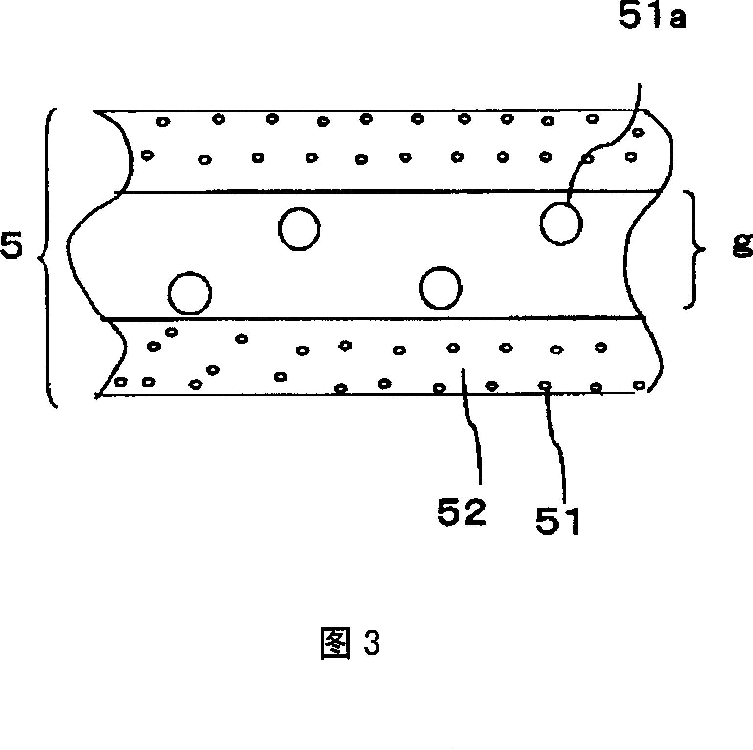
[0302] Then, a band of the resistance heating element was formed with a width of 1.5 mm, and a group of grooves was formed in the band by laser. The group of grooves is formed in the portion of the band located outside the plate-shaped ceramic body. In addition, a sample in which the interval between groups of grooves was changed was produced.
[0303] Moreover, the distance between groups can be divided into each resistance heating element area of the resistance heating element to measure the resistance of each part, and the resistance of each part of each resistance heating element area can be reduced by forming grooves in the part with low resistance and making the resistance larger. . Therefore, the gro...
Embodiment 3
[0311] A silicon carbide sintered body with a thermal conductivity of 80W / (m·K) is ground and processed to produce a plurality of disc-shaped vapor chambers with a plate thickness of 4mm and an outer diameter of 230mm. The insulating layer is attached to the main surface, and the glass paste prepared by kneading ethyl cellulose as a binder and terpineol as an organic solvent with glass powder is laid by screen printing, and the organic solvent is dried by heating at 150°C Thereafter, degreasing treatment was performed at 550° C. for 30 minutes, and firing was performed at a temperature of 700 to 900° C. to form an insulating layer made of glass with a thickness of 200 □. Next, 20% by weight of Au powder, 10% by weight of Pt powder, and 70% by weight of glass were printed in a predetermined pattern shape as conductive materials in order to attach the resistance heating element to the insulating layer. Then, the organic solvent was heated and dried at 150°C, degreased at 450°C f...
PUM
 Abstract
Description
Claims
Application Information