Magnetic thin film, composite magnetic thin film for high frequency and magnetic device using the same

A magnetic thin film and composite magnetic technology, applied in the direction of magnetic thin film, magnetic layer, electrical components, etc., can solve the problems of insufficient specific resistance, increased high-frequency loss, difficulty in applying high-frequency inductors, etc.

Inactive Publication Date: 2006-01-11
TDK CORPARATION
View PDF1 Cites 5 Cited by
  • Summary
  • Abstract
  • Description
  • Claims
  • Application Information

AI Technical Summary

Problems solved by technology

However, the magnetic permeability in the high-frequency band has not been improved, and application to the GHz band cannot be expected.
Moreover, since the specific resistance is not large enough, 100μΩcm or less, the high-frequency loss due to the skin effect increases, and it is difficult to apply to high-frequency inductors

Method used


Image

  • Magnetic thin film, composite magnetic thin film for high frequency and magnetic device using the same
  • Magnetic thin film, composite magnetic thin film for high frequency and magnetic device using the same
  • Magnetic thin film, composite magnetic thin film for high frequency and magnetic device using the same

Examples


Embodiment 1

[0126] The high-frequency magnetic thin film of the present invention was produced according to the following film-forming method.

[0127] (film forming process)

[0128] 100nm thick SiO will be deposited on the Si wafer 2 The material of the film is used as the substrate.

[0129] Using a multi-target sputtering device, a magnetic thin film for high frequency is deposited on a substrate in the following manner. That is to say, the interior of the multi-target sputtering device was pre-evacuated up to 8×10 -5 After Pa, Ar gas was introduced to make the pressure 10 Pa, and a 100 W RF power source was used to sputter etch the substrate surface for 10 minutes.

[0130] Subsequently, the flow rate of Ar gas was adjusted so that the pressure was 0.4Pa, and the Co 87 Zr 5 Nb 8 target, composite target with C (carbon) particles on the Fe target, and Al on the FeCo target 2 o 3 (aluminum oxide) composite target, and deposited (deposited) a composite magnetic thin film as a hi...

Embodiment 2

[0138] (film formation cycle)

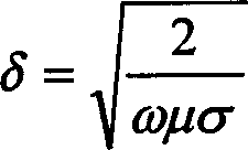
[0139] After depositing a CoZrNb layer with a film thickness of 1.5 nm as the first layer on the substrate, an Fe-C layer with a film thickness of 1.5 nm was formed thereon as the second layer, and this film formation cycle was repeated three times. Next, a FeCoAlO layer having a film thickness of 1.0 nm was deposited on the sixth layer. As above, when three layers of CoZrNb layers and Fe-C layers are stacked alternately, one layer of FeCoAlO layer is deposited, and such a cycle of film-forming treatment is cycled 50 times to obtain a magnetic film with a magnetic film composition as shown in Figure 12. Composite magnetic film (Example 2) (total thickness: 500 nm). In addition, the process flow of film formation is the same as that of the above-mentioned embodiment 1.

Embodiment 3

[0141] (film formation cycle)

[0142] After depositing a CoZrNb layer with a film thickness of 20.0 nm as the first layer on the substrate, an Fe-C layer with a thickness of 5.0 nm was formed thereon as the second layer. Then, a 2.0 nm layer of FeCoAlO was deposited on the Fe-C layer. As above, each layer of CoZrNb layer, Fe-C layer and FeCoAlO layer is alternately deposited, and such a cycle of film-forming treatment is cycled 18 times to obtain a composite magnetic film having the magnetic film composition shown in FIG. 12 (implementation) Example 3) (total thickness: 486 nm). In addition, the process flow of film formation is the same as that of the above-mentioned embodiment 1.


PUM

PropertyMeasurementUnit
thicknessaaaaaaaaaa
thicknessaaaaaaaaaa
thicknessaaaaaaaaaa

Abstract

The invention relates to a high frequency magnetic thin film 1 having both high permeability and high saturation magnetization, which is obtained by combining a T-L composition layer 5 comprising a T-L composition (wherein, T=Fe or FeCo, L=one kind or two or more kinds of C, B and N) and a Co system noncrystalline alloy layer 3 arranged in any one surface side of the T-L composition layer 5. Besides the T-L composition layer 5 and the Co system noncrystalline alloy layer 3, a high resistance layer 7 showing higher electric resistance than the T-L composition layer 5, and the Co system noncrystalline alloy layer 3 is further formed to obtain the high frequency magnetic thin film 1 which has both high permeability and high saturation magnetization and shows high resistance.

Description

technical field [0001] The present invention relates to a magnetic thin film suitable for a gigahertz (GHz) high frequency band and a magnetic element using the magnetic thin film. Background technique [0002] Along with miniaturization and high performance of magnetic elements, magnetic thin film materials having high saturation magnetization and high magnetic permeability in the high-frequency band of the gigahertz band (hereinafter referred to as the GHz band) are required. [0003] For example, monolithic microwave integrated circuits (MMICs), which are in high demand centering on radio transceivers and portable information terminals, are high-frequency integrated circuits composed of active elements such as transistors and circuits. , Resistors, capacitors, inductors and other passive components are produced in batches and integrated on semiconductor substrates such as Si, GaAs, and InP. [0004] On such an MMIC, passive components, especially inductors and capacitors...

Claims


Application Information

Patent Timeline
Patent Type & Authority Applications(China)
IPC IPC(8): H01F10/16H01F10/13H01F17/04H01F17/00H01F41/04H01L27/08
CPCH01F41/046H01L27/08H01F10/16H01F10/132H01F17/0006H01F10/265Y10T428/3183H01F17/04
Inventor 崔京九村濑琢
Owner TDK CORPARATION
Why Eureka
Try Eureka