Optical burst-mode receiver

A receiver, optical burst technology, applied in the field of optical communication, can solve the problems such as the reset pulse signal width is not properly controlled, the preamble time guard band time is increased, the receiving circuit is not stable, etc., to shorten the preamble time, Improved channel utilization and faster charging time

Inactive Publication Date: 2006-02-08
UNIV OF ELECTRONICS SCI & TECH OF CHINA
View PDF0 Cites 6 Cited by
  • Summary
  • Abstract
  • Description
  • Claims
  • Application Information

AI Technical Summary

Problems solved by technology

However, this feedback type reset pulse signal generation circuit has relatively large defects: first, the signal output by the limiting amplifier needs to be input to the envelope detector for envelope detection, so that the required preamble time and guard band time will be different. The second is that relative to the input signal of the entire receiver, the reset pulse signal generated by the feedback reset pulse signal generation circuit has a certain time delay, and the top detection circuit and the bottom detection circuit need to wait for the arrival of the reset pulse signal, thereby The time of the guard band is further increased, thereby reducing the channel utilization rate; the third is figure 2 The width of the reset pulse signal is not properly controlled, so that the overshoot during discharge is more serious, which increases the time of the preamble, thereby further reducing the channel utilization rate; the fourth is that the feedback reset pulse signal generation circuit introduces a feedback mechanism , making the receiving circuit less stable and prone to oscillation

Method used


Image

  • Optical burst-mode receiver
  • Optical burst-mode receiver
  • Optical burst-mode receiver

Examples


Embodiment Construction

[0028] The present invention will be further described below in conjunction with the accompanying drawings and a specific embodiment.

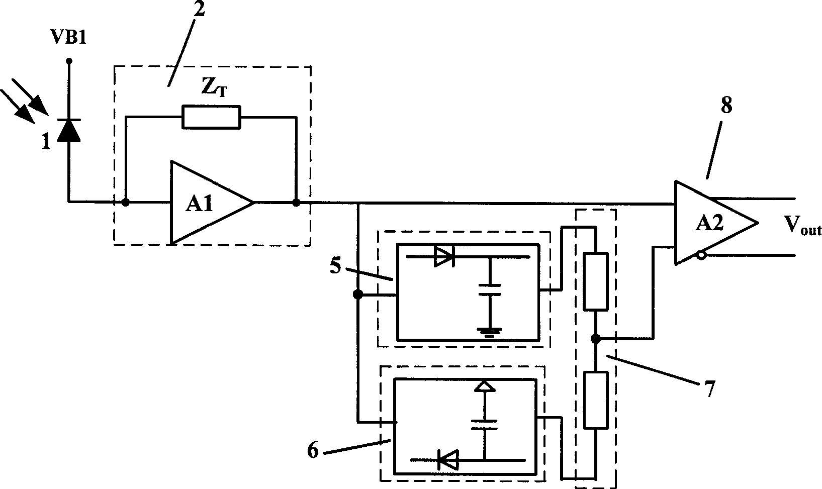
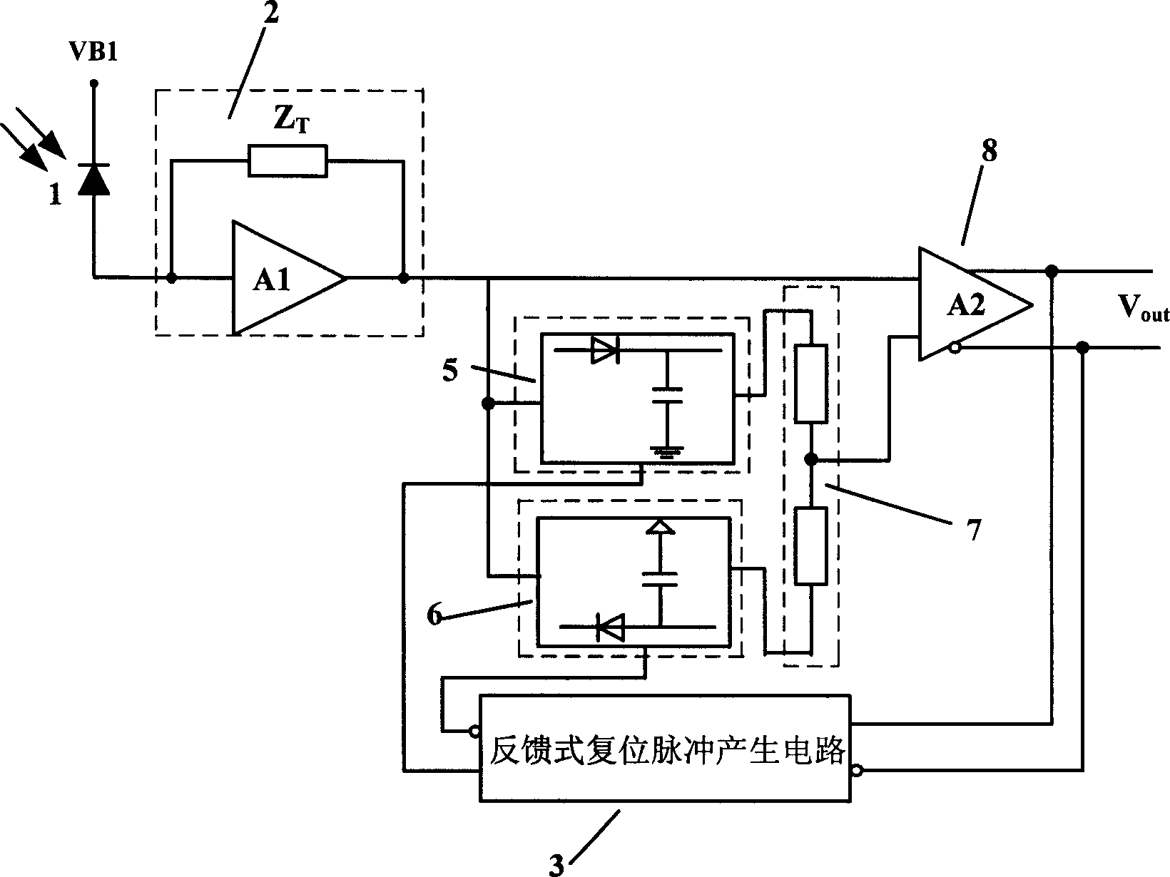
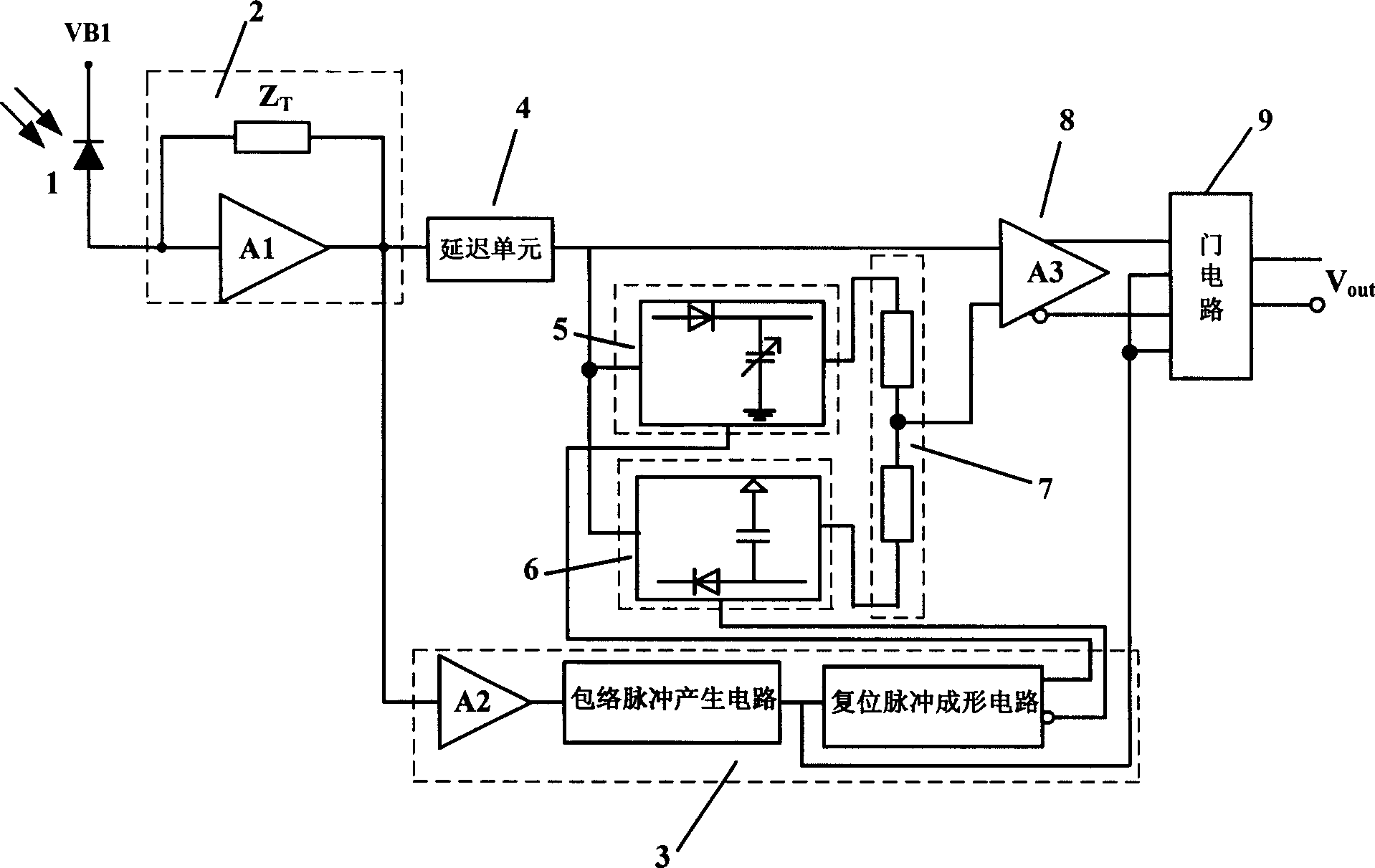
[0029] Figure 4 is a specific embodiment of the present invention, wherein 1 is a photodiode, T1 to T40 are bipolar transistors, R1 to R37 are resistors, DL is a cable delay unit, D1 to D4 are diodes, and M1 to M28 are metal oxide semiconductors Field effect transistor (CMOS tube), VC is a varactor diode, C1 and C4 are capacitors, L1 is an inductor, I1 to I15 are current sources, and VB1 and VC1 are power supplies.

[0030] The circuit composition of the specific embodiment of the present invention is as follows:

[0031] Photodiode 1 is composed of a photodiode; transimpedance preamplifier 2 is composed of bipolar transistors T1 to T6, resistors R1 to R11 and diode D1; feedforward reset pulse signal generating circuit 3 is composed of bipolar transistors T7 to T20 , resistors R12 to R25, metal oxide semiconductor field effect transistors M...


PUM


Abstract

Disclosed is a light bursting receiver, which comprises: photodiode, trans-impedance preamplifier, top and bottom detecting circuits, resistance-type potential divider and limiting amplifier. The invention is characterized in that it also comprises feed-forward reset impulse signal generation circuit, delay unit and gate circuit. Charging capacitor in the top detecting circuit can be variable capacitance; the feed-forward reset impulse signal generation circuit comprises limiting amplifier, an envelope pulse-generating circuit, and a reset pulse shaping circuit. The invention has the advantages of improving usage of signal channel, reducing error codes and of eliminating interference.

Description

technical field [0001] The invention belongs to the technical field of optical communication, and particularly relates to a burst mode optical receiver for identifying and receiving optical digital signals of burst mode and optical digital signals of non-uniform code stream (inhomogeneity of amplitude and packet length). Background technique [0002] Optical fiber communication has developed in an all-round way and has penetrated into various application fields. People are focusing on the key technologies of the next generation optical fiber communication system and broadband optical fiber access network, so that the optical fiber network has both high-speed broadband trunk lines and fast and convenient broadband optical fiber access. to each user. Passive Optical Network (PON, Passive Optical Network) has the advantages of good business transparency, applicable to signals of any standard and rate, anti-electromagnetic interference and easy maintenance. It is a very promisin...

Claims


Application Information

Patent Timeline
Patent Type & Authority Applications(China)
IPC IPC(8): H04B10/158H04B10/66
Inventor 邱琪朱灿
Owner UNIV OF ELECTRONICS SCI & TECH OF CHINA
Why Eureka
Try Eureka