Methods and systems for rapid thermal processing

A high-temperature processing and fast technology, applied in the manufacture of furnaces, electrical components, semiconductors/solid-state devices, etc., can solve the deformation of the wafer, it is difficult to adjust the relative position of the heating unit and the wafer, and it is difficult to achieve uniform temperature distribution on the surface of the wafer And other issues

Inactive Publication Date: 2006-02-15
TAIWAN SEMICON MFG CO LTD
View PDF0 Cites 6 Cited by
  • Summary
  • Abstract
  • Description
  • Claims
  • Application Information

AI Technical Summary

Problems solved by technology

[0005] When the wafer is subjected to rapid high-temperature processing, it is very important to uniformly heat the entire surface of the wafer. The uneven temperature distribution on the surface of the wafer will cause dislocation and distortion of the wafer. However, in the traditional In rapid high temperature processing, it is often difficult to achieve a uniform temperature distribution on the wafer surface, such as figure 1 As shown, it is difficult to adjust the relative position of individual heating units and the wafer, so that the heat energy received by each point on the wafer surface is exactly the same, therefore, a temperature gradient from the edge to the center of the wafer is formed, especially, the wafer Round edges often receive the least amount of thermal energy, as in Figure 2A As shown in Figure 2B, for the peak heating temperature of 1075°C, during the heating cycle, the temperature T1-T3 of the inner ring range is significantly higher than that of the outer ring, and the temperature distribution difference between the inner and outer rings reaches 12°C. In addition, the rapid high temperature Processes are usually operated for short periods of time, for example, about 2-15 minutes. The wafer is rapidly heated to a very high temperature and cooled down rapidly. Subtle differences in thermal energy at different points on the wafer surface can cause significant Therefore, the thermal stress at different points on the wafer surface will ch

Method used


Image

  • Methods and systems for rapid thermal processing
  • Methods and systems for rapid thermal processing
  • Methods and systems for rapid thermal processing

Examples


Embodiment Construction

[0017] In order to make the above-mentioned and other objects, features and advantages of the present invention more comprehensible, the preferred embodiments are listed below, together with the accompanying drawings, and are described in detail as follows:

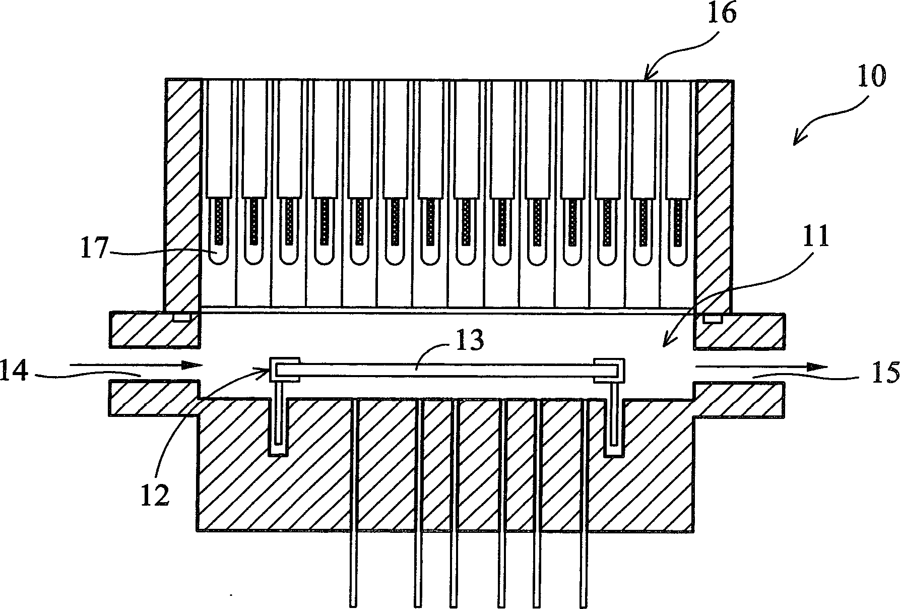
[0018] Since heat conduction is related to the pattern if the pattern on the front side of the semiconductor substrate faces the heat source, it is best to prevent the pattern from being directly irradiated by the heat radiation generated by the heat source.

[0019] The present invention provides methods and systems for rapid high temperature processing of semiconductor substrates. In some embodiments of the present invention, the radiant heat energy is directed to the back side of the semiconductor substrate, while the front side of the semiconductor substrate is not irradiated by the radiant heat energy, so the pattern on the front side of the semiconductor substrate will not affect the uniformity of heat flow. Since t...


PUM


Abstract

Methods for rapid thermal processing of semiconductor substrates are provided. An exemplary method comprises directing radiant heat energy emitted from a heat source toward a backside surface of the semiconductor substrate. Systems for rapid thermal processing also are provided. The effect of the invention is that the heat energy emitted from the heat source is lead to the back of the semiconductor substrate, and the front of the semiconductor is not radiated by the heat energy, so patterns of the front of the semiconductor substrate do not influence evenness of heat flowing, alternatively, a pyrometer is arranged on the front of the semiconductor substrate because the heat source is not set in the front of the semiconductor substrate, by this the real temperature of the front of the semiconductor substrate is exactly measured, and radiation heat energy emitted from the individually heating lamp tube of the heat source is real-time controlled.

Description

technical field [0001] The present invention relates to semiconductor manufacturing process, and in particular to rapid thermal processing (rapid thermal processing), in particular to a method and system for rapid thermal processing of semiconductor substrates. Background technique [0002] Rapid high temperature processing has been widely used in different steps of semiconductor manufacturing process. For example, rapid high temperature processing can be used to deposit different films on semiconductor wafers. Rapid high temperature processing can also be used to implant semiconductor The ions or dopants in the wafer are annealed. Since the operating temperature of the rapid high temperature processing can be rapidly increased or decreased, the required process time is very short and the processing efficiency is also high. [0003] In many rapid high-temperature processing applications, it is often necessary to inject a gas of a specific composition at a specific pressure i...

Claims


Application Information

Patent Timeline
IPC IPC(8): H01L21/02H01L21/30H01L21/324H01L21/20
CPCH01L21/67248F27D99/0006H01L21/67115F27B17/0025F27D5/0037F27D2099/0026
Inventor 麦凯玲杨铭和李资良陈世昌聂俊峰
Owner TAIWAN SEMICON MFG CO LTD
Why Eureka
Try Eureka