Surface mount LED

A technology of LED chips and mounting parts is applied to LEDs. It can solve the problems of inability to apply the optical system, cracks and warping of the resin molding part, and it is difficult to obtain the light distribution characteristics of complete scattering distribution, so as to achieve uniform light distribution characteristics and eliminate the effects of deterioration.

Inactive Publication Date: 2006-03-08
STANLEY ELECTRIC CO LTD
View PDF0 Cites 44 Cited by
  • Summary
  • Abstract
  • Description
  • Claims
  • Application Information

AI Technical Summary

Problems solved by technology

[0014] That is, in LED1, since there is no lamp house, although it is possible to constitute a light source with a so-called complete scattering distribution, when the LED chip 3 to be used becomes large, and when there are a plurality of LED chips 3 to be mounted, the occupation of the LED chip 3 will be limited. The area increases, and due to the stress formed by transparent materials such as epoxy resin constituting the resin molded part 4, the resin molded part 4 will have cracks, warping and other deformations, and it is difficult to guarantee the quality
[0015] Moreover, since the thermal conductivity of the hard substrate 2 is relatively low, the heat generated by the driving of the LED chip 3 is not easily dissipated to the mounting substrate, so the LED chip 3 becomes high temperature, and the luminous efficiency decreases.
[0016] In addition, when the resin molding part 4 is made of epoxy resin, when the LED chip 3 generates short-wavelength light such as ultraviolet rays, the aging of the resin molding part 4 will be accelerated due to the absorption of photons.
[0017] Moreover, in LED5, although the heat generated by the LED chip 3 can be effectively dissipated to the mounting substrate through the lead frame 6, in the manufacturing process, there are processes such as insert molding of the lead frame, welding of the LED chip, and wire bonding. The material of the body 7 requires resins that can be used at high temperatures. Although they have heat resistance such as LCP and PPA as engineering plastics, opaque resins have to be used, so it is difficult to obtain light distribution characteristics with complete scattering distribution. Depending on the situation, it may not be applicable to the specified optical system
[0018] In addition, in LED8, as resins that can perform MID, the above-mentioned LCP, PPA, etc. are used, and similarly depending on the situation, it may not be applicable to a predetermined optical system.

Method used


Image

  • Surface mount LED
  • Surface mount LED
  • Surface mount LED

Examples


Embodiment 1

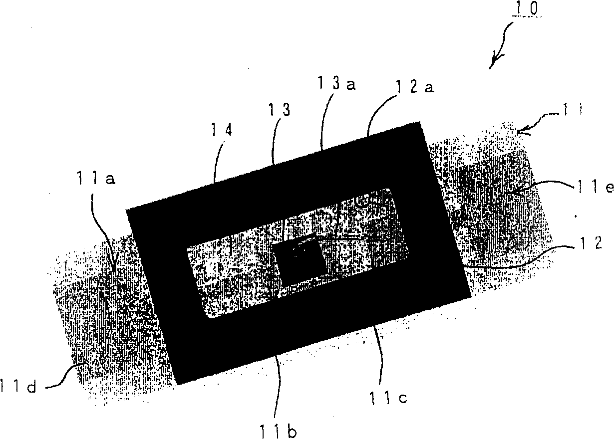
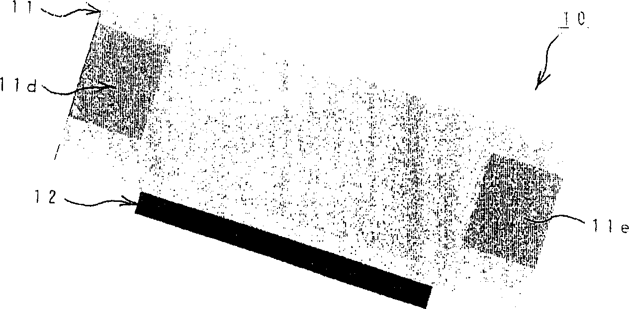
[0056] figure 1 and figure 2 The structure of the first embodiment of the LED of the present invention is shown. exist figure 1 and figure 2 Among them, the LED 10 is composed of the following parts: a silicon substrate 11; a glass frame 12 mounted on the silicon substrate 11; an LED chip 13 mounted on the silicon substrate 11 in the through hole 12a of the glass frame 12; The plastic sealing part 14 in the through hole of the glass frame body 12 .

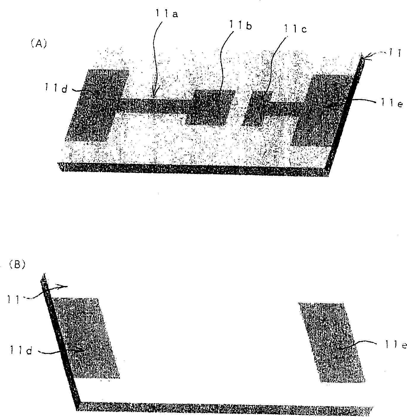
[0057] The above-mentioned silicon substrate 11 is made of plate-shaped silicon, and is formed with a image 3 (A) and image 3 (B) Conductive layer 11a of a predetermined pattern.

[0058] The conductive layer 11a includes an LED chip mounting portion 11b, adjacent connection pads 11c, and electrode portions 11d, 11e surrounding the silicon substrate 11 from both ends to the back surface near the center of the silicon substrate 11.

[0059] The conductive layer 11a is formed, for example, as described below.

[0060] ...

Embodiment 2

[0079] Figure 5 The structure of the second embodiment of the LED of the present invention is shown.

[0080] exist Figure 5 , the structure of LED20 and figure 1 and figure 2 The illustrated LEDs 10 are substantially the same, so the same components are assigned the same symbols and descriptions thereof are omitted.

[0081] The above LED20 with figure 1 and figure 2 Compared with the LED 10 shown, the difference is that the silicon substrate 21 is used instead of the silicon substrate 11 .

[0082] Here, the above-mentioned silicon substrate 21 is made of a slightly thick plate-shaped silicon, and has slopes 21a, 21b that become lower toward the outside at both end edges.

[0083] Such slopes 21a, 21b are formed by, for example, scribing and cutting, or the surface of the silicon substrate 21 is used as (100 plane) and (110 plane) is formed as a slope by, for example, KOH series alkaline wet etching.

[0084] And, for this silicon substrate 21, the conductive la...

Embodiment 3

[0089] Figure 6 The structure of the 3rd embodiment of the LED of this invention is shown.

[0090] exist Figure 6 , the structure of LED30 and figure 1 and figure 2 The illustrated LEDs 10 are substantially the same, so the same components are assigned the same symbols and descriptions thereof are omitted.

[0091] The above LED30 with figure 1 and figure 2 Compared with the LED 10 shown, the difference is that the silicon substrate 31 is used instead of the silicon substrate 11 .

[0092] Here, the silicon substrate 31 is made of silicon, has a trapezoidal gap on the back side, and has spacer surfaces 31a, 31b widening from the center of the back side toward both end edges.

[0093] Such a silicon substrate 31 such as Figure 7 As shown in (A), it consists of a lower part 32 that divides the partition surface into 31a and 31b, and a plate-shaped upper part 33, and is formed by joining the upper part 33 to the upper surface of the lower part 32.

[0094] Here, the...


PUM


Abstract

An LED can include a silicon substrate that has a conductive pattern including an LED chip equipped portion, a connection portion, and external electrodes. A glass frame can be anodic-bonded onto the silicon substrate, and can include a through-hole forming a lamp house. An LED chip can be mounted onto the silicon substrate in the through-hole of the glass frame, and a mold portion made of silicone resin can be filled into the through-hole of the glass frame.

Description

technical field [0001] The invention relates to an LED that uses a transparent resin to plastically seal the surroundings of an LED chip. Background technique [0002] In the past, such LEDs have, for example, Figure 9 ~ Figure 11 structure shown. [0003] That is, first in Figure 9 Among them, the LED1 is composed of the following parts: a hard substrate 2; an LED chip 3 mounted on the hard substrate 2; and a resin molding part 4 formed on the hard substrate 2 and surrounding the LED chip 3. [0004] The above-mentioned hard substrate 2 has a conductive pattern (not shown) forming a predetermined circuit on its surface. Figure 9 (B)). [0005] The above-mentioned LED chip 3 is an LED chip of a known structure, and is soldered to the chip mounting portion of the above-mentioned hard substrate 2, and is wire-bonded (not shown) to adjacent connection pads (not shown). Moreover, the above-mentioned resin molding part 4 is made of a transparent material such as epoxy resi...

Claims


Application Information

Patent Timeline
Patent Type & Authority Applications(China)
IPC IPC(8): H01L33/00H01L33/50H01L33/56H01L33/64
CPCH01L33/486H01L33/641H01L33/62H01L2224/48091H01L2224/48465H01L2224/48227H01L2224/45144H01L2924/01322H01L2924/00014H01L2924/00
Inventor 东海林巌
Owner STANLEY ELECTRIC CO LTD
Why Eureka
Try Eureka