Process for mfg. one-dimensional X ray refracted diffraction micro structural component of polymethyl methyl acrylate material

A technology of polymethyl methacrylate and production method, applied in X-ray/γ-ray/particle irradiation therapy, analyzing materials, material analysis using wave/particle radiation, etc., can solve the problem of low depth of device structure and surface roughness It can achieve the effect of small material limitation, good focal spot quality, and reduced X-ray absorption.

Inactive Publication Date: 2006-06-14
乐孜纯
View PDF0 Cites 4 Cited by
  • Summary
  • Abstract
  • Description
  • Claims
  • Application Information

AI Technical Summary

Problems solved by technology

[0005] The purpose of the present invention is to solve the problems of low device structure depth, large material restrictions, and high roughness in the existing manufacturing technology, and provide a polymethyl methacrylate with large device structure depth, small material restrictions, and low surface roughness. Fabrication method of material one-dimensional X-ray diffraction microstructure device

Method used


Image

  • Process for mfg. one-dimensional X ray refracted diffraction micro structural component of polymethyl methyl acrylate material

Examples


Embodiment 1

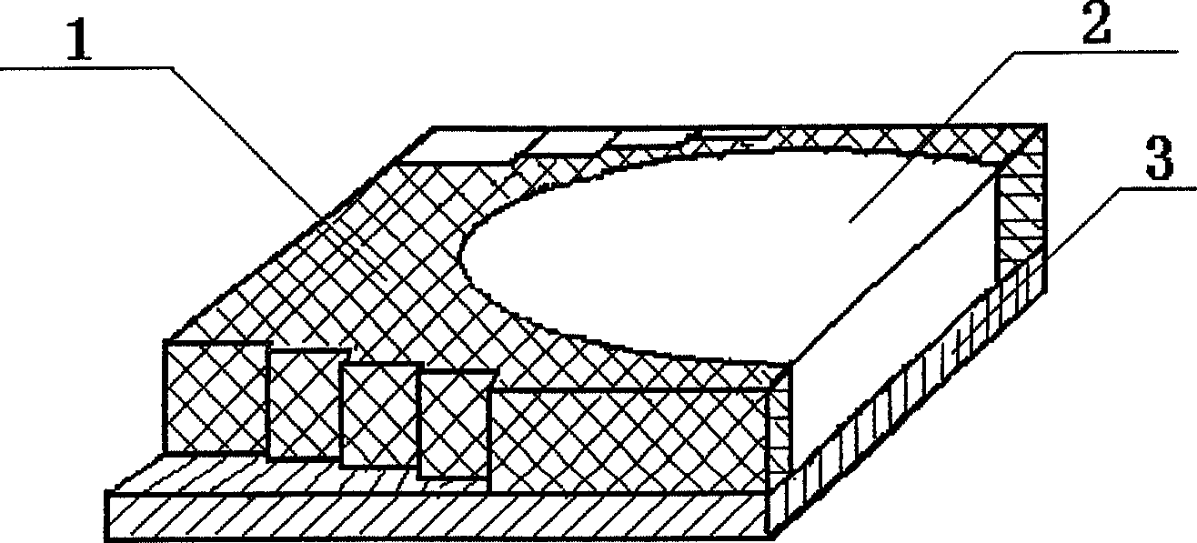
[0029] Referring to accompanying drawing 1, a kind of manufacturing method of polymethyl methacrylate material one-dimensional X-ray diffraction microstructure device, described one-dimensional X-ray diffraction microstructure device comprises a plurality of lens units arranged coaxially in sequence , the lens unit is composed of a lens composed of a main body with an air gap, the upper side wall of the lens main body has upward stepped steps, and the step width of each step is equal; the lower side of the lens main body The wall is provided with a downward step-like step symmetrically arranged with the axis as the center line and the step of the upper side wall of the lens. The lens is provided with an open air gap. The maximum diameter of the gap corresponding to the direction of the minor axis of the ellipse is smaller than the minor axis of the ellipse, and the major axes of the elliptical air gaps of the lens unit are located on the same straight line. The manufacturing me...

Embodiment 2

[0044] In the technical scheme of the present embodiment, the thickness of the polyimide material is 5 microns in the step (C), and the metal material electroforming cathode film described in the step (D) is a titanium material, and the surface of the titanium sheet is coated with The thickness of coating polymethyl methacrylate is 500 microns, and all the other steps are identical with embodiment 1.

Embodiment 3

[0046] In the technical scheme of the present embodiment, the metal material electroforming cathode film described in the step (D) is a titanium material, and the thickness is 400 nanometers, and the thickness of the polymethyl methacrylate coated on the surface of the titanium sheet is 800 nm in the step (K). Micron, all the other steps are the same as in Example 1.


PUM

PropertyMeasurementUnit
thicknessaaaaaaaaaa
thicknessaaaaaaaaaa
thicknessaaaaaaaaaa

Abstract

The invention relates to poly methyl methacrylate material one dimension X ray diffraction refraction microstructure device manufacturing method. It includes the following steps: making photolithography mask edition; processing silicon substrate; coating polyimide and baking and solidifying; producing metallic film to use as electro forming cathode; coating thick photoresist; exposing, developing, and hardening; producing metallic film to use as X ray photolithography mask absorbent; removing the photoresist an electro forming cathode; back photoengraving and silicon corroding; making titanium slice as supporting; coating poly methyl methacrylate, backing, and solidifying; X ray photoengraving and developing.

Description

(1) Technical field [0001] The invention relates to an X-ray microstructure optical device, especially a manufacturing process of a microstructure X-ray optical device based on dual effects of refraction and diffraction, which is suitable for one-dimensional X-ray refraction and diffraction microstructure devices made of polymethyl methacrylate organic materials production occasions. (2) Technical background [0002] X-ray composite lens is an X-ray microstructure optical device based on refraction effect proposed by A. Snigirev in 1996, which is suitable for high-energy X-ray band (that is, X-ray radiation energy exceeds 5keV). It has the advantages of no need to bend the optical path, good high temperature stability and easy cooling, simple and compact structure, and low requirements on the surface roughness of the lens. It has broad application prospects in the field of ultra-high resolution X-ray diagnostic science and technology. In recent years, research on various X...

Claims


Application Information

Patent Timeline
Patent Type & Authority Applications(China)
IPC IPC(8): G02B3/00A61N5/10G01N23/083G03F7/20
Inventor 乐孜纯梁静秋董文全必胜
Owner 乐孜纯
Why Eureka
Try Eureka