Method of chemical gas phase precipitation for growing carbon doped silicon germanium alloy buffer layer and germanium film

A technology of chemical vapor deposition and buffer layer, which is applied in the direction of gaseous chemical plating, metal material coating process, coating, etc., which can solve the complex process, high cost, and high requirements for precise control of reaction gas source flow, etc. question

Inactive Publication Date: 2006-07-12
NANJING UNIV
View PDF0 Cites 7 Cited by
  • Summary
  • Abstract
  • Description
  • Claims
  • Application Information

AI Technical Summary

Problems solved by technology

However, this method has high requirements on the precise control of the flow rate of the reaction gas source, and the process is complicated and the cost is high.

Method used


Image

  • Method of chemical gas phase precipitation for growing carbon doped silicon germanium alloy buffer layer and germanium film
  • Method of chemical gas phase precipitation for growing carbon doped silicon germanium alloy buffer layer and germanium film
  • Method of chemical gas phase precipitation for growing carbon doped silicon germanium alloy buffer layer and germanium film

Examples


Embodiment Construction

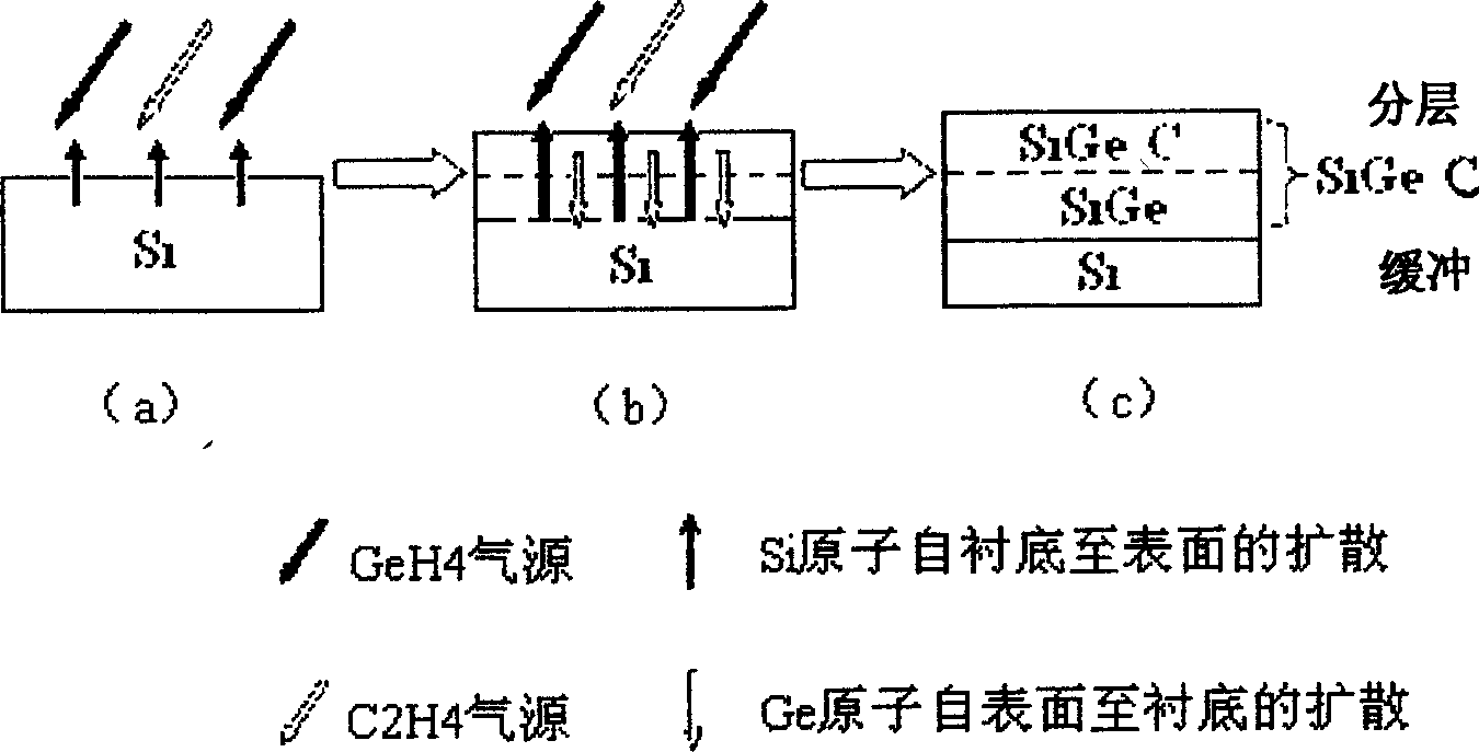
[0016] figure 1 In, for Si 1-x Ge x The growth process of the :C buffer layer is described as follows: on the sample surface, Si and reaction gas source (GeH 4 、C 2 h 4 ) react to form Si 1-x Ge x :C film, the higher growth temperature causes the Si atoms in the substrate to diffuse to the surface, thus maintaining the Si on the surface of the sample 1-x Ge x : The progress of C thin film epitaxial growth (such as figure 1 (a) shown); at the same time, Si 1-x Ge x : Metal Ge atoms in the C epitaxial layer diffuse toward the substrate to fill the vacancies left by the diffusion of Si to the surface, so the CVD epitaxial Si 1-x Ge x : Form Si under C thin film 1-x Ge x layer (eg figure 1 (b) shown). As a result of the above growth process, Si with Ge composition gradient is obtained on the Si substrate. 1-x Ge x :C buffer layer (such as figure 1 (c) shown).

[0017] The present invention adopts CVD method, growth uses germane (GeH 4 ) as germanium source, eth...


PUM

PropertyMeasurementUnit
thicknessaaaaaaaaaa

Abstract

The invention relates to a chemical gas phase deposition growth carbon germanium-silicon alloy isolating switch and growth germanium thin film method, which uses GeH4, C2H4 as reacting gas at 700-850 deg. and 10-100Pa compression intensity, wherein the C2H4 divider board is 0.01-0.15 Pa; the GeH4 divider board 0.10-1.10 Pa; the gas souse reactes with Si to combine the Ge of the epitaxial layer so that it generates a layer of Ge component anamorphic Si1-xGex: C buffer layer on the substrate surface with the thickness 0.5-10 micrometer; and then it generates Ge thin film especially at 400-600 deg and 15-100Pa compression intensity, wherein the GeH4 divider board is 0.07-1.11Pa.

Description

1. Technical field [0001] The present invention relates to adopting the chemical vapor deposition (CVD) method to prepare the carbon-doped silicon-germanium alloy (Si) with germanium (Ge) composition gradient on Si substrate 1-x Ge x :C) buffer layer, followed by Si 1-x Ge x : Method for epitaxial growth of single crystal Ge film on C buffer layer. 2. Background technology [0002] As the first-generation semiconductor material, Ge has the advantage of high carrier mobility compared to Si; epitaxially grow Ge and Si with high Ge composition on Si 1-x Ge x Alloy, can be used for Si with high cut-off frequency (>100G Hz) 1-x Ge x Fabrication and research of novel devices such as / Si heterojunction bipolar transistors and long-wavelength photodetectors. [0003] There is a 4.2% lattice mismatch and a 5.6% thermal mismatch between Ge and Si. The Ge thin film obtained directly on the Si substrate has high density of structural defects, poor single crystal and photoelect...

Claims


Application Information

Patent Timeline
Patent Type & Authority Applications(China)
IPC IPC(8): C23C16/06C23C16/52
Inventor 韩平王荣华夏冬梅刘成祥谢自力赵红修向前朱顺明顾书林施毅张荣郑有炓
Owner NANJING UNIV
Why Eureka
Try Eureka