Semiconductor device, its manufacturing method, and electronic device

A technology of electronic equipment and semiconductors, applied in semiconductor/solid-state device manufacturing, circuits, transistors, etc., can solve problems that cannot be used in practice

Inactive Publication Date: 2006-07-19
SHARP KK +2
View PDF3 Cites 76 Cited by
  • Summary
  • Abstract
  • Description
  • Claims
  • Application Information

AI Technical Summary

Problems solved by technology

However, as described above, field effect transistors provided with a protective layer cann

Method used


Image

  • Semiconductor device, its manufacturing method, and electronic device
  • Semiconductor device, its manufacturing method, and electronic device
  • Semiconductor device, its manufacturing method, and electronic device

Examples


no. 1 Embodiment approach

[0081] Regarding the first embodiment of the present invention, based on FIGS. Figure 5 It will be explained as follows.

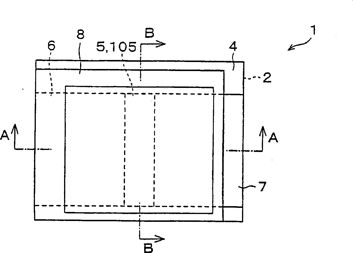
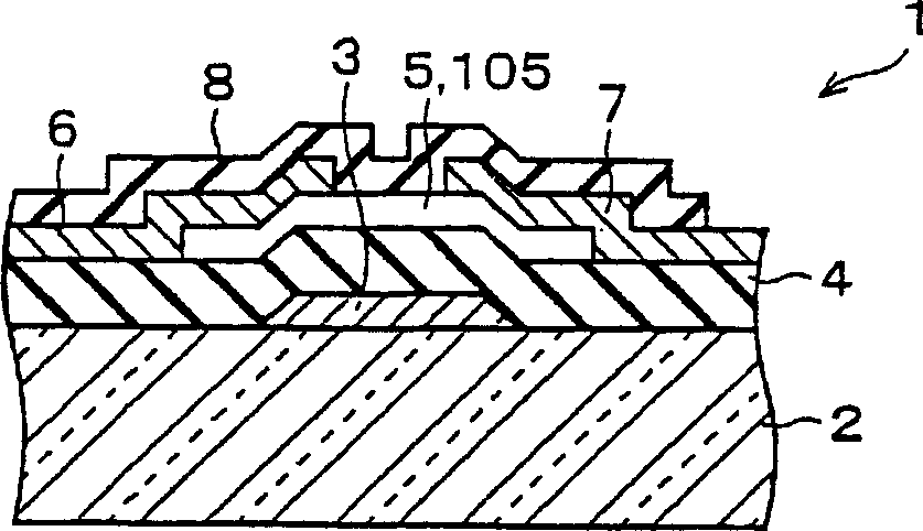
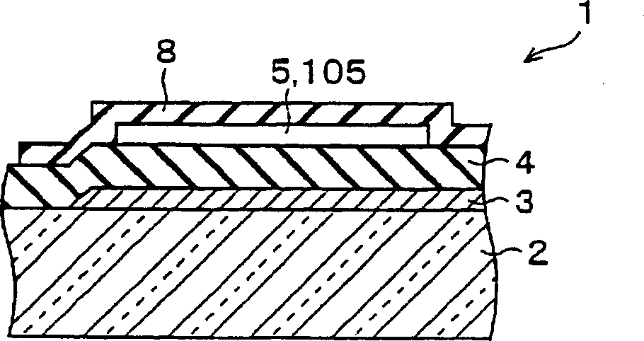
[0082] FIG. 1( a ) shows a plan view of a thin film transistor 1 of this embodiment. Moreover, FIG. 1( b ) shows a sectional view taken along the line A-A of FIG. 1( a ), and FIG. 1( c ) shows a sectional view taken along the line B-B of FIG. 1( a ). In addition, in FIG. 1( a ), for the sake of simplification of the drawing, the description of the unevenness in the central part of the surface of the protective layer 8 shown in FIG. 1( b ) and FIG. 1( c ) is omitted.

[0083] Such as Figure 1(a) ~ Figure 1(c) As shown, in a thin film transistor 1 as a semiconductor device, a gate electrode 3 is formed on an insulating substrate 2, a semiconductor layer 5 is laminated on the gate electrode 3 via a gate insulating layer 4, and an electrode part is formed on the semiconductor layer 5. The source electrode 6 and the drain electrode 7 are formed, and the pr...

no. 2 Embodiment approach

[0104] The second embodiment of the present invention will be described as follows based on FIGS. 6 to 8 .

[0105] FIG. 6( a ) shows a plan view of the thin film transistor 11 of this embodiment. And Fig. 6 (b) shows the sectional view of the C-C line arrow direction of Fig. 6 (a), and Fig. 6 (c) shows the sectional view of the D-D line arrow direction of Fig. 6 (a). In addition, in FIG. 6( a ), for the sake of simplification of the drawing, the description of the irregularities in the central portion of the surface of the protective layer 19 shown in FIGS. 6( b ) and 6( c ) is omitted.

[0106] Such as Figure 6(a) ~ Figure 6(c) As shown, in a thin film transistor 11 as a semiconductor device, a source electrode 14 and a drain electrode 15 are formed on an insulating base layer 13 formed on an insulating substrate 12 except for intervals, and a semiconductor layer 16 and a gate insulating layer 17 are sequentially stacked on them. and the gate electrode 18 , and further fo...

no. 3 Embodiment approach

[0130] About 3rd Embodiment of this invention, if it demonstrates based on FIGS. 9-11, it will be as follows.

[0131] FIG. 9( a ) shows a plan view of the thin film transistor 21 of this embodiment. Moreover, FIG. 9( b ) shows a cross-sectional view in the arrow direction of E-E line in FIG. 9( a ), and FIG. 9( c ) shows a cross-sectional view in the arrow direction of line F-F in FIG. 9( a ).

[0132] Figure 9(a) ~ Figure 9(c) As shown, in a thin film transistor 21 as a semiconductor device, a source electrode 24 and a drain electrode 25 are formed on an insulating base layer 23 formed on an insulating substrate 22 , and a semiconductor layer 26 and a first gate insulating layer 27 are formed thereon. The semiconductor layer 26 and the first gate insulating layer 27 are covered with the second gate insulating layer 28 , and the second gate insulating layer 28 also serves as a protective layer for the semiconductor layer 26 . A gate electrode 29 is formed on the second gat...


PUM


Abstract

A thin film transistor (1) wherein a gate electrode (3) is formed on an insulative substrate (2), a gate insulating layer (4) is formed on the gate electrode (3), a semiconductor layer (5) is formed on the gate insulating layer (4), a source electrode (6) and a drain electrode (7) are formed on the semiconductor layer (5), and a protective layer (8) covering them are formed. The semiconductor layer (5) is isolated from the atmosphere. The semiconductor layer (5) (active layer) is formed of a ZnO polycrystalline semiconductor doped with, for example, a group V element. Since the surface state of the ZnO semiconductor is reduced thanks to the protective layer (8) and inward expansion of the depletion layer is prevented, the ZnO semiconductor is of an n-type showing its intrinsic resistance value and contains excessive free electrons. The added element acts as acceptor impurities in the ZnO semiconductor, decreasing the excessive electrons. Thus the gate voltage to eliminate the excessive free electrons lowers, thereby making the threshold voltage around 0 V. A semiconductor device using a zinc oxide for an active layer and having a protective layer for isolating the active layer from the atmosphere can be actually used.

Description

technical field [0001] The present invention relates to a semiconductor device having a zinc oxide-based active layer, a semiconductor device suitable for a switching element used in an electronic device, and an electronic device using the semiconductor device. Background technique [0002] Conventionally, zinc oxide (ZnO) is a semiconductor that is transparent in the visible light region and exhibits relatively good physical properties even when manufactured at a low temperature. Therefore, studies have been actively conducted in recent years, and various technical reports have been made. [0003] For example, in terms of academics, papers in Documents 1 to 3 have been published. These papers all indicate that a thin film transistor using ZnO as an active layer can operate with good performance. [0004] Patent Document 1: R.L.Hoffman, B.J.Norris and J.F.Wager, "ZnO-based transparent thin-film transistors" APPLIED PHYSICS LETTERS VOLUME 82, NUMBER5, 3 FEBRUARY 2003, PP733...

Claims


Application Information

Patent Timeline
IPC IPC(8): H01L21/336H01L29/786
Inventor 杉原利典大野英男川崎雅司
Owner SHARP KK
Why Eureka
Try Eureka