Semiconductor device manufacturing method

A manufacturing method, semiconductor technology, applied in semiconductor/solid-state device manufacturing, transistors, electrical components, etc., can solve problems such as short life span of capacitors, insulation damage of capacitor insulating film 54, unstable film thickness, etc., and achieve the effect of preventing insulation damage

Inactive Publication Date: 2006-08-30
SANYO ELECTRIC CO LTD
View PDF1 Cites 2 Cited by
  • Summary
  • Abstract
  • Description
  • Claims
  • Application Information

AI Technical Summary

Problems solved by technology

[0011] Therefore, then as Figure 10 As shown, even if the upper electrode layer 55 is formed to form a capacitor, as described above, since the film thickness of the capacitor insulating film 54 has a thin part, and the film thickness is not stable, there is a possibility that electric field concentration occurs and this part is likely to occur. Dielectric breakdown of the capacitor insulating film 54 and short life of the capacitor

Method used


Image

  • Semiconductor device manufacturing method
  • Semiconductor device manufacturing method
  • Semiconductor device manufacturing method

Examples


Embodiment Construction

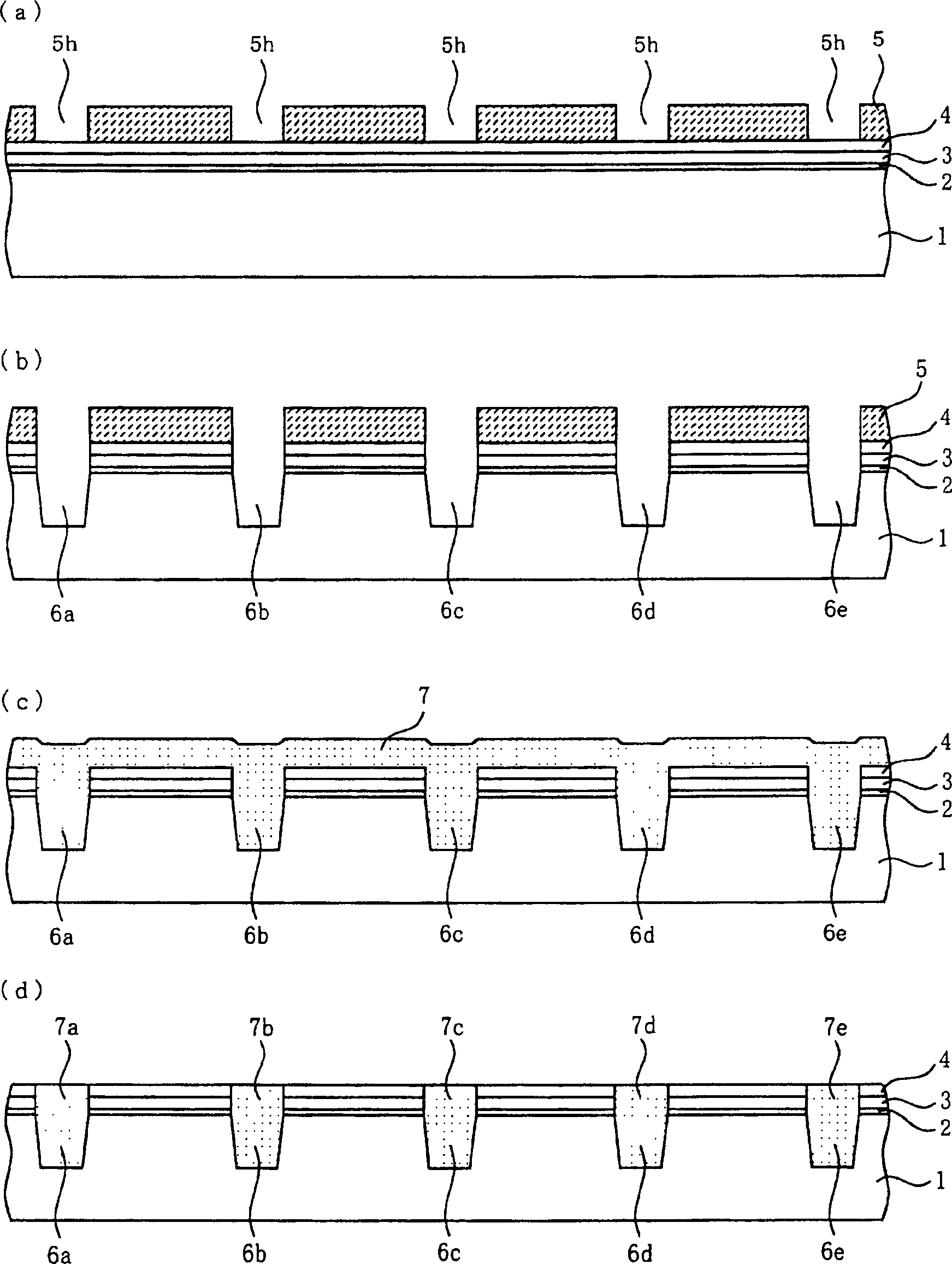
[0079] Next, a method of manufacturing a semiconductor device according to a first embodiment of the present invention will be described with reference to the drawings.

[0080] Such as figure 1 (a), by performing thermal oxidation, SiO is formed on the surface of the P-type silicon substrate 1 2 Membrane 2 (Silicon Dioxide Membrane). Then, using CVD method on SiO 2 On the film 2, a polysilicon film 3 (Poly Silicon film) having a film thickness of about 50 nm, a Si film having a film thickness of 120 nm, and 3 N 4 Film 4 (silicon nitride film). And then in Si 3 N 4 A photoresist layer 5 having a plurality of openings 5h is formed on the film 4 .

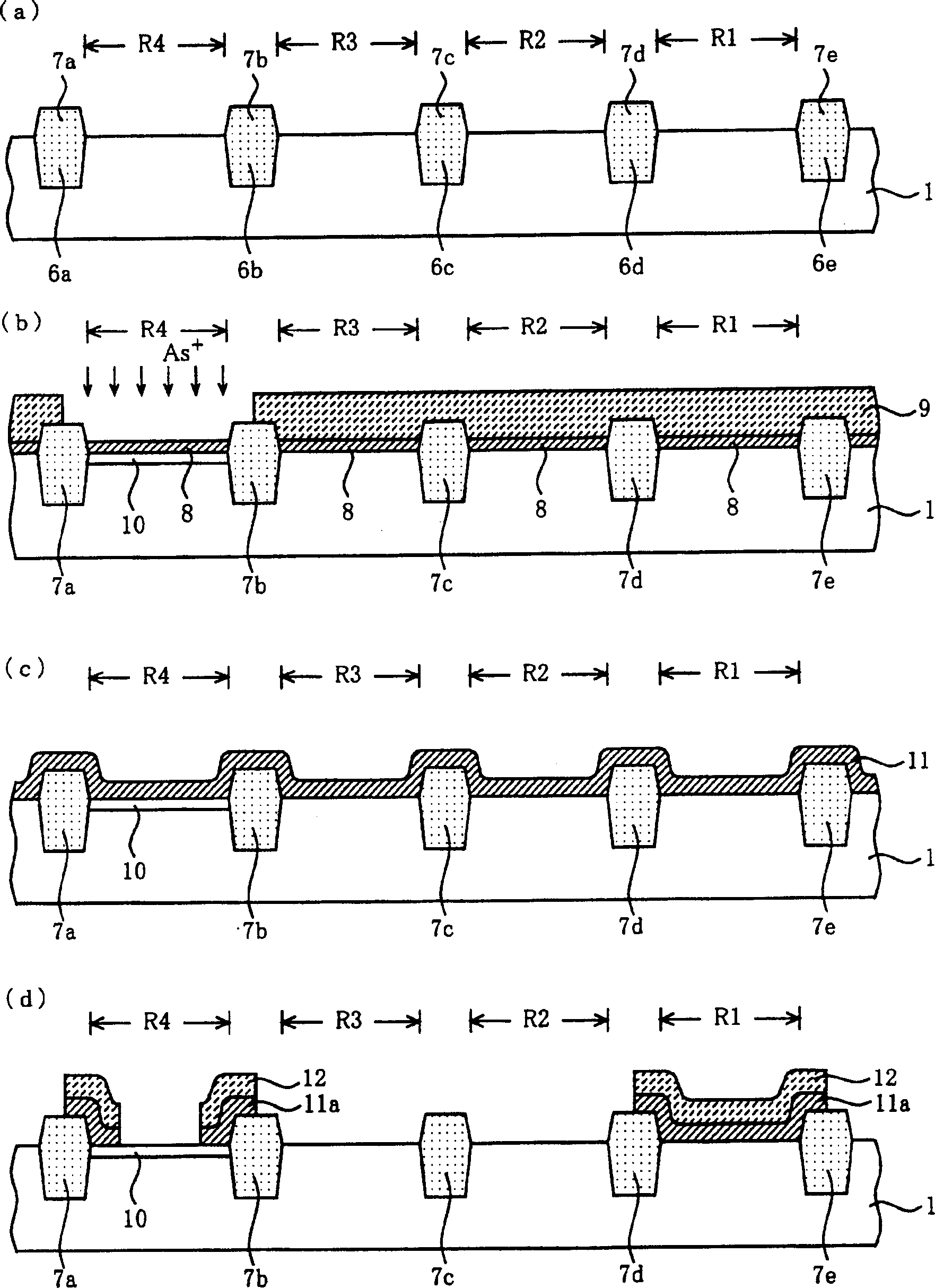
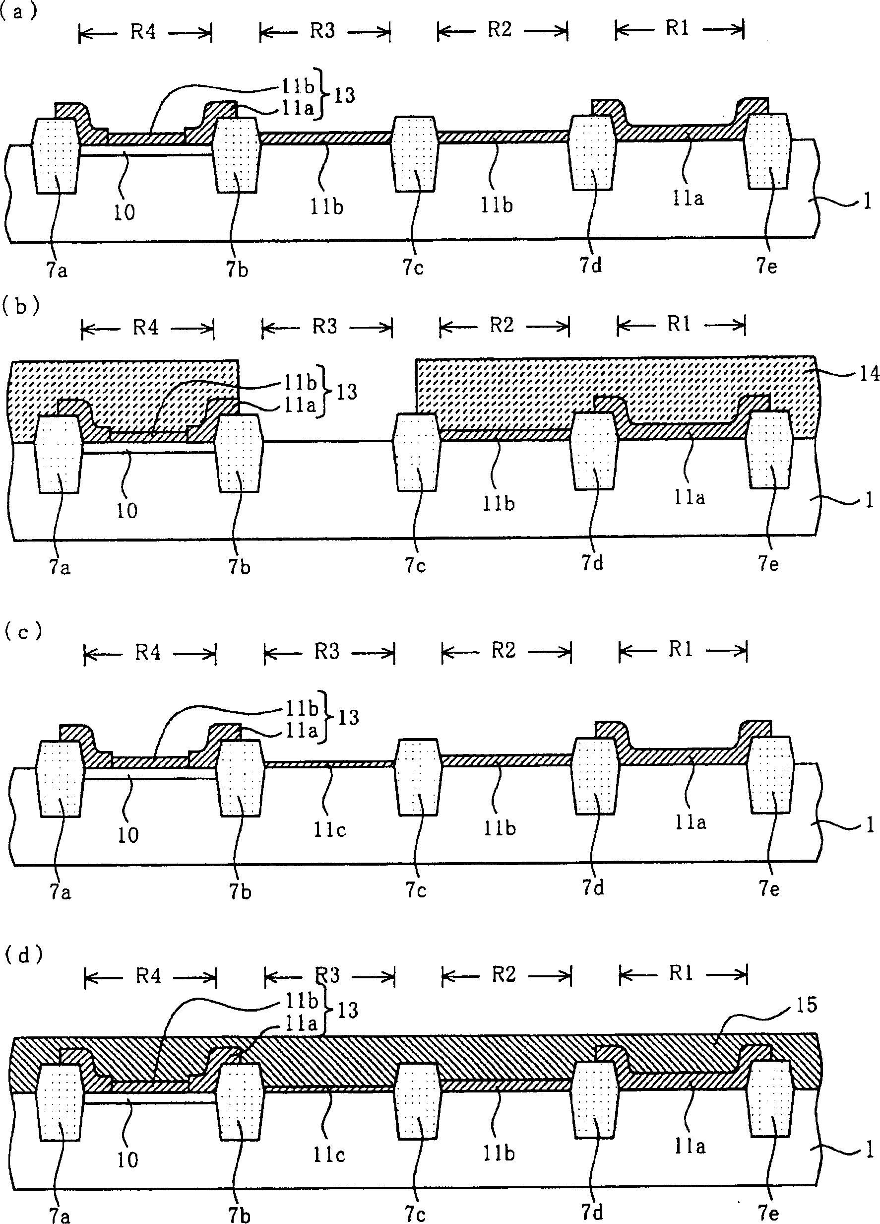
[0081] Secondly, if figure 1 As shown in (b), using the photoresist layer 5 having a plurality of openings 5h as a mask, the Si exposed at the openings 5h are sequentially etched. 3 N 4 Film 4, polysilicon film 3, SiO 2 film 2, and then etch the surface of the P-type silicon substrate 1 to form trenches 6a, 6b, 6c, 6d, 6...


PUM


Abstract

The invention is to prevent dielectric breakdown of a capacitor in a semiconductor device having the capacitor and a MOS transistor formed on a same semiconductor substrate. A SiO2 film that is to be a gate insulation film of a high voltage MOS transistor is formed on a whole surface of a P-type semiconductor substrate. A photoresist layer is selectively formed in a high voltage MOS transistor formation region and on a part of a SiO2 film covering edges of trench isolation films adjacent to a capacitor formation region, and the SiO2 film is removed by etching using this photoresist layer as a mask. Since the photoresist layer functions as a mask in this etching, the edges of the trench isolation films adjacent to the capacitor are not cut too deep. The SiO2 film remaining in this etching and a SiO2 film to be formed thereafter form a capacitor insulation film.

Description

technical field [0001] The present invention relates to a method of manufacturing a semiconductor device, and more particularly to a method of manufacturing a semiconductor device having a capacitor and a MOS transistor on the same semiconductor substrate. Background technique [0002] Currently, a semiconductor device having a MOS transistor and a capacitor is known. On the other hand, with the high integration of semiconductor devices in recent years, the shallow trench isolation method (hereinafter referred to as STI method) is widely used instead of the local oxidation method (LOCOS) for the isolation of active regions. The STI method refers to filling shallow trenches in a semiconductor substrate with an insulating material such as silicon dioxide by high-density plasma chemical vapor deposition (HDPCVD), and using it as a field insulating film. [0003] Next, a method of manufacturing a semiconductor device having a capacitor and a high withstand voltage MOS transisto...

Claims


Application Information

Patent Timeline
Patent Type & Authority Applications(China)
IPC IPC(8): H01L21/8234
CPCH01L27/0629H01L28/40H01L21/823462
Inventor 藤岛达也福田干夫塚田雄二绪方敬士饭田伊豆雄
Owner SANYO ELECTRIC CO LTD
Why Eureka
Try Eureka