Semiconductor device, substrate for mounting semiconductor chip, processes for their production, adhesive, and double-sided adhesive film
An adhesive, adhesive film technology, applied in the direction of film/sheet adhesive, adhesive type, semiconductor devices, etc., can solve the problem of cracks, unusable, thermal expansion coefficient of semiconductor chips and printed wiring boards big difference
- Summary
- Abstract
- Description
- Claims
- Application Information
AI Technical Summary
Problems solved by technology
Method used
Image

Examples
Embodiment 1
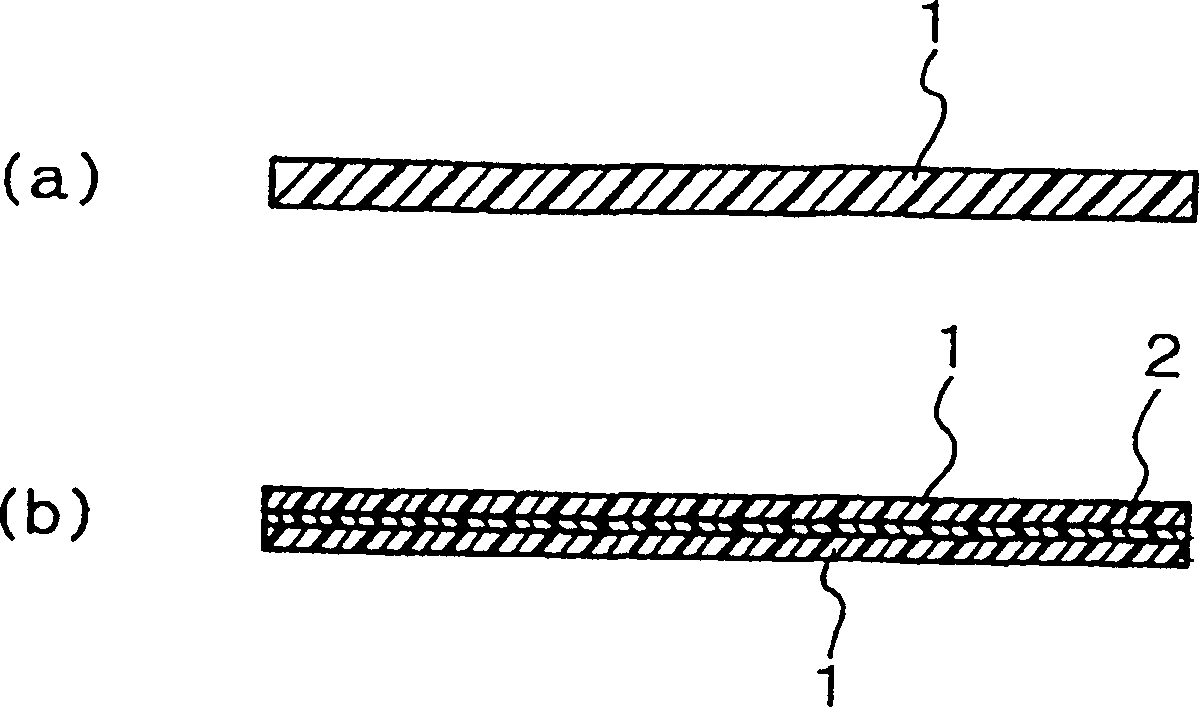
[0144] figure 1 (a) is a cross-sectional view of a single-layer thermosetting adhesive film, which is composed of a thermosetting adhesive 1 and its cured product is determined by a dynamic viscoelasticity measuring device at 25° C. The elastic modulus 10 is defined as the range of 2000 MPa, and , The modulus of elasticity at 260° C. is specified in the range of 3-50 MPa, and the semi-cured state is at the level of 10-40% of the total curing heat generation when measured by DSC (differential calorimeter). An epoxy group-containing acrylic copolymer film in which the amount of solvent remaining in the thermosetting adhesive film is dried to 2% or less is used.
[0145] figure 1 (b) shows a cross-sectional view of a three-layer adhesive film in which a thermosetting adhesive 1 is applied to both sides of a polyimide film 2 . In this example, U-pilex (trade name) with a thickness of 50 micrometers manufactured by Ube Industries was used as the polyimide film.
[0146] figure...
Embodiment 2
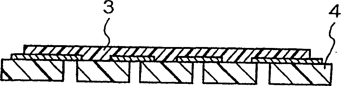
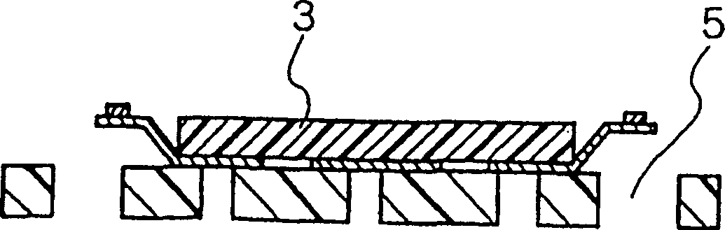
[0157] Figure 7 The manufacturing steps of the semiconductor mounting substrate and the semiconductor device are shown.
[0158] The thermosetting adhesive tape (adhesive member) 3 made of thermosetting adhesive 1 is cut into a prescribed size ( Figure 7 (a)). The cured product of thermosetting adhesive 1 has an elastic modulus of 10-2000 MPa at 25°C measured with a dynamic viscoelasticity measuring device, and an elastic modulus of 3-50 MPa at 260°C. The semi-cured state is about 10 to 40% of the total curing heat generation.
[0159] On the surface of the polyimide wax substrate 5 where one layer of Cu wiring is applied and the inner lead portion and the through hole for the external solder terminal are formed as in the TAB tape, the cut thermosetting adhesive tape 3 is precisely aligned. Afterwards, carry out hot pressing with hot press machine, obtain the substrate for semiconductor mounting ( Figure 7 (b)).
[0160] In this example, a multi-connected semiconductor...
Embodiment 3
[0180] As the epoxy resin, 45 parts by weight of bisphenol A type epoxy resin (epoxy equivalent 200, produced by Yuhua Shell Epoxy Co., Ltd.) 45 parts by weight; cresol novolak type epoxy resin (epoxy equivalent 220 , ESCN001) 15 weight parts that Sumitomo Chemical Industry Co., Ltd. produces; As epoxy resin solidifying agent, use novolak type epoxy resin (プリイオ-fen LF2882 that Dainippon Ink Chemical Industry Co., Ltd. produces) 40 weight parts; Have miscibility with epoxy resin and the high molecular weight resin of weight-average molecular weight more than 30,000 is used, phenoxy resin (molecular weight 50,000, the フェノト-トYP-50 that Dongdu Chemical Co., Ltd. produces) 15 parts by weight; As Epoxy-containing acrylic rubber, use 150 parts by weight of epoxy-containing acrylic rubber (molecular weight 1,000,000, HTR-860-P3 produced by Imperial Chemical Industry Co., Ltd.); as curing accelerator, use curing accelerator 1-cyanoethyl -2-phenylimidazole (キュゾ-ル 2PZ-CN) 0.5 parts by we...
PUM
| Property | Measurement | Unit |
|---|---|---|
| Elastic modulus | aaaaa | aaaaa |
| Elastic modulus | aaaaa | aaaaa |
| Elastic modulus | aaaaa | aaaaa |
Abstract
Description
Claims
Application Information
 - R&D
- Intellectual Property
- Life Sciences
- Materials
- Tech Scout
- Unparalleled Data Quality
- Higher Quality Content
- 60% Fewer Hallucinations
Browse by: Latest US Patents, China's latest patents, Technical Efficacy Thesaurus, Application Domain, Technology Topic, Popular Technical Reports.
© 2025 PatSnap. All rights reserved.Legal|Privacy policy|Modern Slavery Act Transparency Statement|Sitemap|About US| Contact US: help@patsnap.com