Semiconductor device, adhesive, and double-sided adhesive film

一种粘合剂、粘合膜的技术,应用在粘合剂类型、半导体器件、薄膜/薄片状的粘合剂等方向,能够解决耐湿性试验劣化大、产生裂缝、不能使用等问题

Inactive Publication Date: 2010-05-12
RESONAC CORPORATION
View PDF11 Cites 0 Cited by
  • Summary
  • Abstract
  • Description
  • Claims
  • Application Information

AI Technical Summary

Problems solved by technology

[0015] In the case of mounting a semiconductor chip on a printed wiring board using these adhesives, which are printed wiring board related materials, the difference in thermal expansion coefficient between the semiconductor chip and the printed wiring board is large, and cracks will be generated during reflow , so you cannot use
In addition, it cannot be used because of the large deterioration in the humidity resistance test under severe conditions such as a temperature cycle test or PCT treatment.

Method used


Image

  • Semiconductor device, adhesive, and double-sided adhesive film
  • Semiconductor device, adhesive, and double-sided adhesive film
  • Semiconductor device, adhesive, and double-sided adhesive film

Examples


Embodiment 1

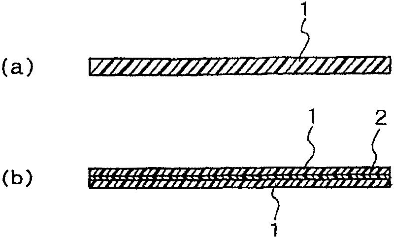
[0144] figure 1 (a) is a cross-sectional view of a single-layer thermosetting adhesive film, which is composed of a thermosetting adhesive 1 and its cured product is determined by a dynamic viscoelasticity measuring device at 25° C. The elastic modulus 10 is defined as the range of 2000 MPa, and , the modulus of elasticity at 260°C is specified in the range of 3-50MPa, and the semi-cured state is 10-40% of the total curing heat when measured by DSC (differential calorimeter). Use the thermosetting adhesive film inside Epoxy-containing acrylic copolymer films with residual solvent content dried to less than 2%.

[0145] figure 1 (b) shows a cross-sectional view of a three-layer adhesive film in which a thermosetting adhesive 1 is applied to both sides of a polyimide film 2 . In this example, as the polyimide film, a 50-micron-thick ユ-ピレ produced by Ube Industries was used. ツ クス (trade name).

[0146] figure 2 It is a cross-sectional view of a substrate for mounting a semi...

Embodiment 2

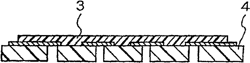
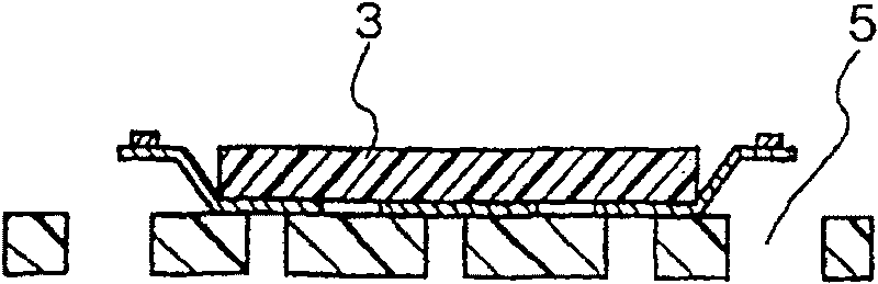
[0157] Figure 7 The manufacturing steps of the semiconductor mounting substrate and the semiconductor device are shown.

[0158] The thermosetting adhesive tape (adhesive member) 3 made of thermosetting adhesive 1 is cut into a prescribed size ( Figure 7 (a)). The cured product of thermosetting adhesive 1 has an elastic modulus of 10-2000 MPa at 25°C measured with a dynamic viscoelasticity measuring device, and an elastic modulus of 3-50 MPa at 260°C. The semi-cured state is about 10 to 40% of the total curing heat generation.

[0159] On the surface of the polyimide wax substrate 5 where one layer of Cu wiring is applied and the inner lead portion and the through hole for the external solder terminal are formed as in the TAB tape, the cut thermosetting adhesive tape 3 is precisely aligned. Afterwards, carry out hot pressing with hot press machine, obtain the substrate for semiconductor mounting ( Figure 7 (b)).

[0160] In this example, a multi-connected semiconductor...

Embodiment 3

[0189] As the epoxy resin, 45 parts by weight of bisphenol A type epoxy resin (epoxy equivalent 200, produced by Yuhua Shell Epoxy Co., Ltd.) 45 parts by weight; cresol novolak type epoxy resin (epoxy equivalent 220 , ESCN001 produced by Sumitomo Chemical Industry Co., Ltd.) 15 parts by weight; As the epoxy resin curing agent, use novolak type epoxy resin (プリイオ-フライリ-フリリ-フリオ-フ produced by Dainippon Ink Chemical Industry Co., Ltd. エ NF2882) 40 parts by weight; As a high molecular weight resin with compatibility with epoxy resin and weight average molecular weight more than 30,000, phenoxy resin (molecular weight 50,000, produced by Dongdu Chemical Co., Ltd. エ ノト-トYP-50) 15 parts by weight; As epoxy-containing acrylic rubber, use epoxy-containing acrylic rubber (molecular weight 1,000,000, the HTR-860-P3 that Imperial Chemical Industry Co., Ltd. produces) 150 parts by weight; As curing Accelerator, use curing accelerator 1-cyanoethyl-2-phenylimidazole (キ エ アゾ-ル 2PZ-CN) 0.5 parts...


PUM

PropertyMeasurementUnit
glass transition temperatureaaaaaaaaaa
tensile modulusaaaaaaaaaa
glass transition temperatureaaaaaaaaaa

Abstract

The invention aims at improving the temperature resisting cycle characteristics after mounting and moisture absorption resiting reflow characteristics of a chip-mounted semiconductor, and provides anadhesive which functions as a bonding member to be used when a semiconductor chip is mounted on an organic supporting substrate and which has storage moduli at 25 DEG C and at 260 DEG C as measured with a dynamic visco-elasticity measuring instrument of 10-2000 MPa and 3-50 MPa, respectively, a double-coated adhesive film produced therewith, a semiconductor device, an semiconductor chip mounting substrate, and methods of manufacturing these products.

Description

[0001] This application is an application with the application number "97199604.0", the filing date is October 8, 1997, and the title of the invention is "semiconductor device, semiconductor chip mounting substrate, their manufacturing method, adhesive and double-sided adhesive film" division case. technical field [0002] The present invention relates to a semiconductor device, a manufacturing method thereof, a substrate for mounting a semiconductor chip suitable for use in the manufacture of the semiconductor device, a manufacturing method thereof, an adhesive, and a double-sided adhesive film. Background technique [0003] In recent years, with the miniaturization of electronic equipment and the high frequency of work, the semiconductor packages that load them are required to be mounted on the substrate at high density. With the progress of miniaturization and light weight, people have developed an array of external terminal areas. Small packages called micro BGA (Ball Gr...

Claims


Application Information

Patent Timeline
Patent Type & Authority Patents(China)
IPC IPC(8): C09J163/00C09J7/00H01L23/12
CPCH01L2224/92247H01L2224/45124H01L24/45H01L24/50H01L2224/83101H01L2224/48227H01L24/83H01L24/29H01L2924/15311H01L2924/01029H01L2224/83192H01L2924/01012H01L2224/73265H01L2224/32225H01L24/73H01L2224/2612H01L2224/45H01L2224/45144H01L2224/50H01L2924/15183H01L2924/181H01L2924/351H01L2924/00H01L2924/00012H01L2924/00014H01L2924/3512H01L23/12
Inventor 山本和德岛田靖神代恭稻田祯一栗谷弘之金田爱三富山健男野村好弘细川羊一桐原博景山晃
Owner RESONAC CORPORATION
Why Eureka
Try Eureka