Semiconductor device, adhesive and adhesive film

An adhesive and semiconductor technology, applied in the direction of adhesive types, semiconductor devices, film/sheet-like adhesives, etc., can solve the problems of large deterioration of moisture resistance test, cracks, and unusable use.

Inactive Publication Date: 2006-12-06
HITACHI CHEM CO LTD
View PDF6 Cites 0 Cited by
  • Summary
  • Abstract
  • Description
  • Claims
  • Application Information

AI Technical Summary

Problems solved by technology

[0015] In the case of mounting a semiconductor chip on a printed wiring board using these adhesives, which are printed wiring board related materials, the difference in thermal expansion coefficient between the semiconductor chip and the printed wiring

Method used


Image

  • Semiconductor device, adhesive and adhesive film
  • Semiconductor device, adhesive and adhesive film
  • Semiconductor device, adhesive and adhesive film

Examples


Embodiment 1

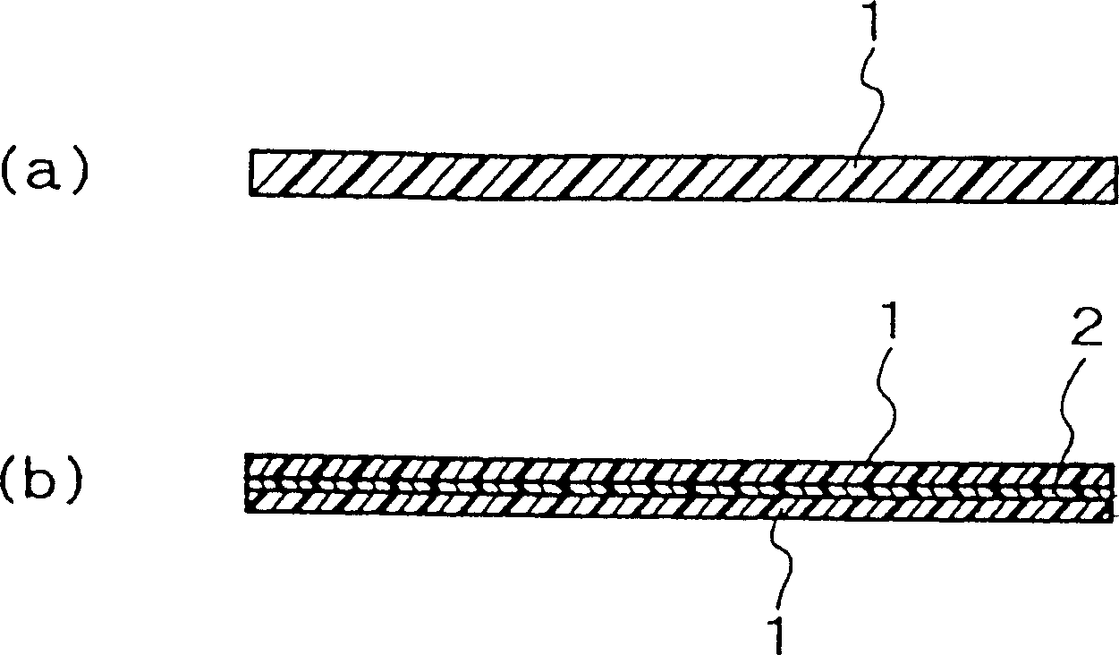
[0144] figure 1 (a) is a cross-sectional view of a single-layer thermosetting adhesive film, which is composed of a thermosetting adhesive 1 . The elastic modulus of the cured product measured with a dynamic viscoelasticity measuring device at 25°C is specified as 10-2000MPa, and the elastic modulus at 260°C is specified as 3-50MPa, which is in the range of exothermic heat. A semi-cured state at the level of 10 to 40% of the total curing calorific value when measured by DSC (differential calorimeter). An epoxy group-containing acrylic copolymer film in which the amount of solvent remaining in the thermosetting adhesive film is dried to 2% or less is used.

[0145] figure 1 (b) shows a cross-sectional view of a three-layer adhesive film in which a thermosetting adhesive 1 is applied to both sides of a polyimide film 2 . In this example, as the polyimide film, Ube Industries, Ltd. UPILEX (trade name) with a thickness of 50 micrometers was used.

[0146] figure 2 It is a cr...

Embodiment 2

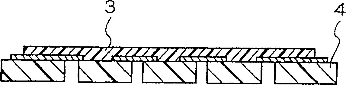
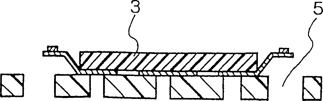
[0157] Figure 7 The manufacturing steps of the semiconductor mounting substrate and the semiconductor device are shown.

[0158] The thermosetting adhesive tape (adhesive member) 3 made of thermosetting adhesive 1 is cut into a prescribed size ( Figure 7 (a)). The cured product of thermosetting adhesive 1 has an elastic modulus of 10-2000 MPa at 25°C measured with a dynamic viscoelasticity measuring device, and an elastic modulus of 3-50 MPa at 260°C. The semi-cured state is about 10 to 40% of the total curing heat generation.

[0159] On the surface of the polyimide film substrate 5 on which one layer of Cu wiring is applied and the same inner lead portion and through-holes for external solder terminals as the TAB tape are formed, the cut thermosetting adhesive tape 3 is precisely aligned. , carry out hot pressing with hot press machine, obtain the substrate for semiconductor mounting ( Figure 7 (b)).

[0160] In this example, a set of frame substrates for semiconduct...

Embodiment 3

[0180] As epoxy resin, use 45 parts by weight of bisphenol A type epoxy resin (epoxy equivalent 200, EPIKOTE 828 produced by YukaShell Epoxy Co., Ltd.); cresol novolak type epoxy resin (epoxy equivalent 220, Sumitomo Chemical Industry Co., Ltd. produces ESCN001) 15 weight parts; As epoxy curing agent, use 40 weight parts of novolac type epoxy resin (PLYOPHENLF2882 produced by Dainippon Ink Chemical Industry Co., Ltd.); Solubility and the high molecular weight resin of weight-average molecular weight more than 30,000, use 15 parts by weight of phenoxy resin (molecular weight 50,000, PHENOTOHTO YP-50 produced by Dongdu Chemical Co., Ltd.); as epoxy-containing acrylic rubber, use Epoxy acrylic rubber (molecular weight 1,000,000, the HTR-860-P3 that Imperial Chemical Industry Co., Ltd. produces) 150 weight parts; As curing accelerator, use curing accelerator 1-cyanoethyl-2-phenylimidazole (CUREZOLE 2PZ -CN) 0.5 parts by weight; as a silane coupling agent, use 0.7 parts by weight o...


PUM

PropertyMeasurementUnit
Elastic modulusaaaaaaaaaa

Abstract

The present invention aims at an improvement in temperature-cycle resistance after packaging in semiconductor devices and also an improvement in moisture-absorbed reflow resistance, and provides an adhesive having a storage elastic modulus at 25°C of from 10 to 2,000 MPa and a storage elastic modulus at 260°C of from 3 to 50 MPa as measured with a dynamic viscoelastic spectrometer, and also a double-sided adhesive film, a semiconductor device and a semiconductor chip mounting substrate which make use of the adhesive, and their production process.

Description

[0001] This application was filed by Hitachi Chemical Industry Co., Ltd. on October 8, 1997, the application number is 97199604.0, and the title of the invention is "semiconductor device, substrate for semiconductor chip mounting, their manufacturing method, adhesive and double-sided adhesive film "A divisional application of the invention patent application. technical field [0002] The present invention relates to a semiconductor device and an adhesive and an adhesive film suitable for use in the manufacture of the above semiconductor device. Background technique [0003] In recent years, with the miniaturization of electronic equipment and the high frequency of work, the semiconductor packages that load them are required to be mounted on the substrate at high density. With the progress of miniaturization and light weight, people have developed an array of external terminal areas. Small packages called micro BGA (Ball Grid Array)...

Claims


Application Information

Patent Timeline
IPC IPC(8): H01L21/50H01L21/58H01L21/56H01L21/60C09J7/00C09J163/00H01L23/13H01L23/31H01L23/498
CPCH01L23/13H01L2924/07802H01L2924/01006H01L2224/83101H01L2224/48227H01L24/32H01L2924/15311H01L2924/12044H01L2924/15159H01L2924/01012H01L2224/48091H01L24/45C09J163/00H01L23/49816H01L2924/01047H01L2924/01079H01L23/49827H01L2924/01013H01L2224/83192H01L2924/10253H01L2924/01078H01L2924/01051H01L2924/15184H01L2924/01045H01L24/29H01L2924/01039H01L24/83H01L23/3128H01L2224/45124H01L2924/12041H01L2924/01087H01L2924/01082H01L2224/92247H01L24/50H01L2924/01027H01L2224/83856H01L2924/01015H01L2924/01005H01L2924/01033H01L2924/01019H01L2224/45144H01L2924/0102H01L2224/32225H01L2924/014H01L24/48H01L2924/01014H01L2224/73265H01L2924/01077H01L2924/0105H01L2924/01023H01L2224/2919H01L2924/01029H01L2924/0665H01L24/73H01L24/86H01L2224/2612H01L2924/15787H01L2924/181H01L2924/351Y10T428/28Y10T428/2848Y10T428/2852Y10T428/287Y10T428/31511Y10T428/31515H01L2924/00014H01L2924/00H01L2924/3512H01L2924/00012
Inventor 山本和德岛田靖神代恭稻田祯一栗谷弘之金田爱三富山健男野村好弘细川羊一桐原博景山晃
Owner HITACHI CHEM CO LTD
Why Eureka
Try Eureka