High-frequency clock jitter measuring circuit and calibration method thereof

A technology for measuring circuits and high-frequency clocks, applied in the direction of measuring electricity, measuring electrical variables, frequency measuring devices, etc., can solve the problem that the clock cannot be used in measuring jitter circuits, achieve fast and efficient delay adjustment, avoid errors, and be easy to use Effect

Inactive Publication Date: 2006-09-27
PEKING UNIV SHENZHEN GRADUATE SCHOOL
View PDF0 Cites 14 Cited by
  • Summary
  • Abstract
  • Description
  • Claims
  • Application Information

AI Technical Summary

Problems solved by technology

[0006] The main purpose of the present invention is to provide a kind of high-frequency clock jitter measurement circuit for the shortcoming that the previous self-built in-chip measurement jitter circuit cannot be applied to very high frequency (as above 1 GHz) clock measurement, and the period error (period jitter) is used as The size of the jitter of the measured clock, so that the timing jitter of the high-frequency phase-locked loop can be measured without an external reference clock

Method used


Image

  • High-frequency clock jitter measuring circuit and calibration method thereof
  • High-frequency clock jitter measuring circuit and calibration method thereof
  • High-frequency clock jitter measuring circuit and calibration method thereof

Examples


specific Embodiment 1

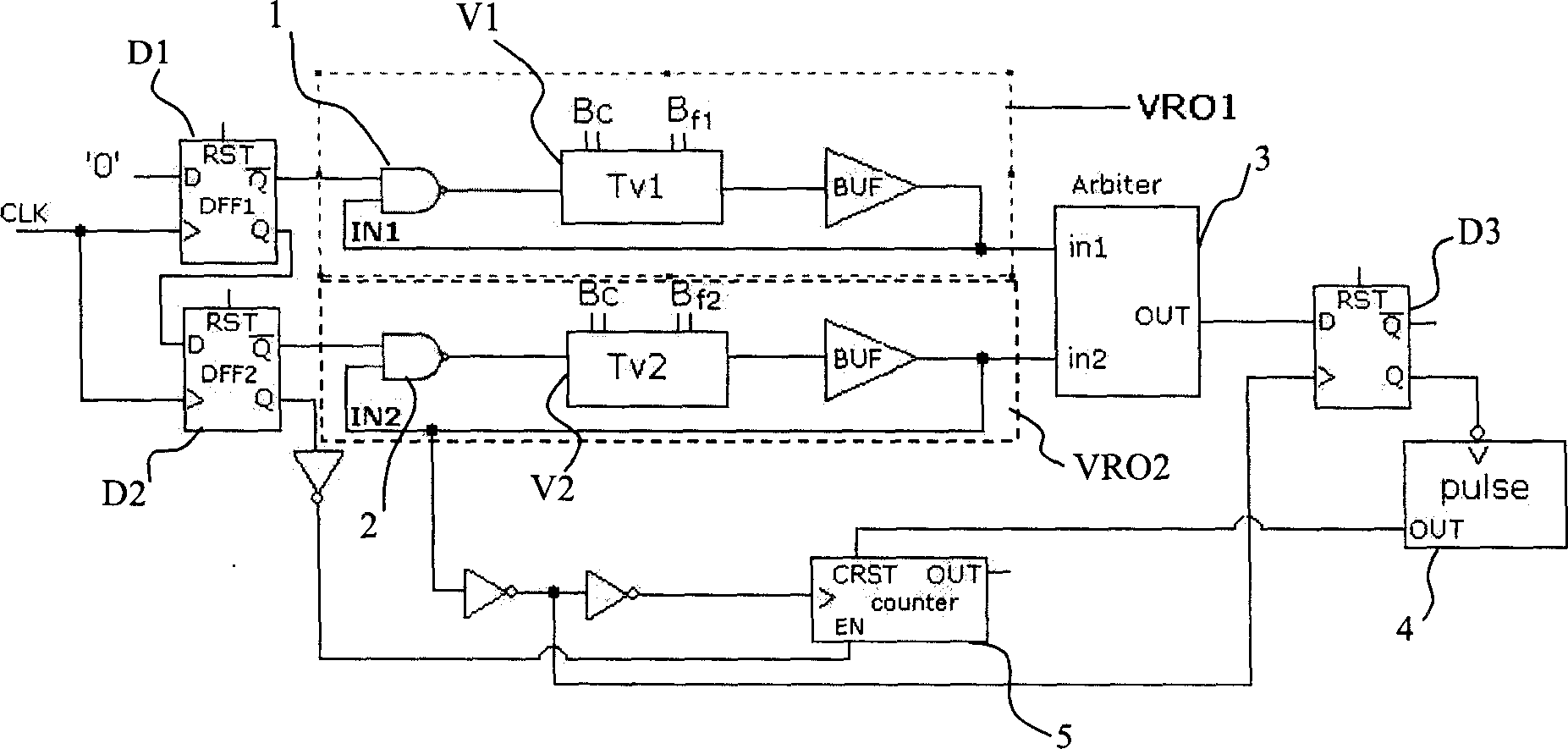
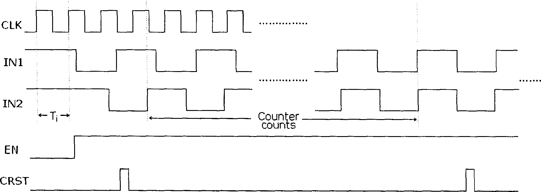
[0055] Specific embodiment one, such as figure 1 Shown is the overall structure diagram of the jitter measurement. The jitter measurement circuit mainly includes: a first oscillation signal generation unit, a second oscillation signal generation unit, a first reset control unit and a first counting unit.

[0056] The first oscillating signal generation unit includes the first D flip-flop D1 and the first ring oscillator VRO1 connected in series, the first ring oscillator VRO1 includes the first NAND gate 1 and the first ring oscillator V1 as the first opening module, the first The input terminal of a D flip-flop D1 inputs a low level, the clock input terminal inputs the measured clock signal CLK, and the first NAND gate 1 responds to the negative output terminal output signal of the first D flip-flop D1 and the first oscillation signal in1 respectively, The output end is coupled to the first ring oscillator V1, and the first ring oscillator V1 generates and outputs a first osc...

specific Embodiment 2

[0069] Embodiment 2. The difference from Embodiment 1 is that the output terminals of the first and second ring oscillators are additionally connected with a buffer drive BUF, in order to reduce the impact of the load circuit on the ring oscillator frequency.

specific Embodiment 3

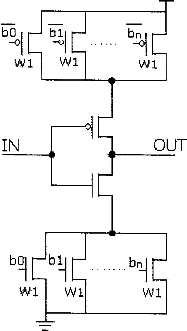
[0070] Specific Embodiment 3. On the basis of specific embodiments 1 and 2, the ring vibration is improved, and the ring vibration adopts a differential control method. One disadvantage of the original vernier caliper type TDC is that it occupies a relatively large area, and the higher the accuracy, the larger the area.

[0071] In this method, the first and second ring oscillators are composed of an odd number of inverter delay units to form a feedback closed loop. In order to make the oscillation frequency variable, the delay amount of the inverter delay unit is designed to be controllable. In order to facilitate The system is compatible with the digital system, and this control adopts the digital control method.

[0072] Traditional inverter delay units such as image 3 As shown, the number of PMOS and NMOS transistors that are turned on is selected through the control word B, so as to control the current when the inverter level jumps, and then control the delay of the inver...


PUM


Abstract

This invention relates to a high-frequency clock jitter measuring circuit and calibration method thereof, which comprises a first/second oscillation signal unit to generate the first/second oscillation signal with TV1/TV2 period (TV1 G01R 29/02 G01R 23/02 G01R 31/00 H03K 5/19 6 13 4 2006/4/18 1837835 2006/9/27 100501423 2009/6/17 2009/6/17 2009/6/17 Peking University Shenzhen Graduate School 518057 Zhang Jingkai Li Chongren Yu Fei Tian Chao guo yan 44223

Description

【Technical field】 [0001] The invention belongs to self-built in-chip measurement (BIST) technology, and relates to a high-frequency clock jitter measurement circuit, a jitter measurement circuit with a calibration function and a calibration method thereof. 【Background technique】 [0002] Phase-locked loops and frequency synthesis circuits composed of phase-locked loops play a pivotal role in today's high-frequency digital field. Timing stability is a key parameter for systems with frequencies above GHz. A major source of noise in high-frequency digital communication systems is clock phase distortion, which can be measured as timing jitter. In recent years, the measurement of system timing jitter has received more and more attention. [0003] The traditional method of measuring chip timing jitter is off-chip measurement, that is, the clock output pin of the chip is connected to an external related instrument to measure and analyze the timing jitter. However, the performanc...

Claims


Application Information

Patent Timeline
Patent Type & Authority Applications(China)
IPC IPC(8): G01R29/02G01R23/02G01R31/00H03K5/19
Inventor 张靖恺李崇仁余菲田超
Owner PEKING UNIV SHENZHEN GRADUATE SCHOOL
Why Eureka
Try Eureka